 |
||
|
||
| ||
|
||
|
||
| ||
We proceed with the analysis of the most important characteristics of high-performance DDR2 memory modules using our RightMark Memory Analyzer. Today we are going to review a new offer from Corsair — high-speed DDR2-800 memory modules with SPD EPP support (Enhanced Performance Profiles) and extremely low latencies — 2GB dual-channel kit of XMS2-6400C3 memory modules. Manufacturer InformationModule manufacturer: Corsair Memory Module ExteriorPhoto of the memory module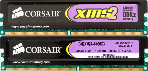
Module Part NumberModule Part Number Expansion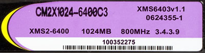
The manufacturer's web site does not publish the DDR2 Part Number expansion of XMS2-series memory modules. TWIN2X2048-6400C3 Specs run that this product is a kit of two modules, 2GB in total, based on sixteen 64M x 8 chips. These modules support the new open EPP standard (SPD extension), developed by Corsair and NVIDIA. It allows to configure memory modules for maximum performance automatically on motherboards that support this standard. The manufacturer guarantees operation of these modules in DDR2-800 mode with EPP 3-4-3-9-2T timings and 2.2 V voltage. But the default mode in the standard SPD section is the standard DDR2-800 mode with 5-5-5-18 timings. SPD chip dataDescription of the general SPD standard: Description of the specific SPD standard for DDR2:
Data of the "standard" SPD section are usual for Corsair modules. The fastest mode these modules are capable of is characterized by the cycle time of 2.5 ns (400 MHz, DDR2-800). This mode corresponds to the first supported tCL = 5, the full timings scheme is written as 5-5-5-18, which agrees with the official characteristics from the datasheet. Reduced CAS# latency (CL X-1 = 4) corresponds to the non-standard cycle time of 3.7 ns, that is approximately 270 MHz. It probably means DDR2-533 mode and the cycle time of 3.75 ns. Nevertheless, the incorrect cycle time results in fractional timings, which can be written (rounded to one figure after the dot) as 4-3.4-3.4-12.2. This scheme will most likely be rounded up by most BIOS's to 4-4-4-13. Nevertheless, DDR2-533 mode has grown outdated long ago for high-speed DDR2 modules, so these values hardly make sense — it would have been reasonable to remove them from SPD. Manufacturer’s JEDEC ID Code and Part Number of the modules are correct. Interestingly, these modules also contain information about their manufacturing date (Week 17, 2006). Nevertheless, their serial number is still missing. Let's review the most important data from the "non-standard" SPD section that corresponds to EPP profiles, represented by Bytes 99-127. EPP Standard Description:
You can see that our modules support the EPP standard and contain information on two full profiles (or four abbreviated profiles that lack most latency and voltage tweaks for various signal lines). The first profile (Profile 0) is considered to be optimal (recommended as a default profile). It corresponds to the 2.5ns cycle time (DDR2-800 mode). But unlike the standard SPD section, EPP Profile 0 for this mode specifies 3-4-3-8.8 timings (rounded up to 3-4-3-9), 2T address command rate and 2.2 V voltage, as well as other tweaks (timings and voltages), which are not published in the table. The second EPP profile (Profile 1) corresponds to DDR2-1066 mode with the 1.875ns cycle time. Corresponding timings are also fractional - 5-5.06-5.06-14.93. Motherboards with EPP support should detect this scheme as 5-5-5-15. Address command rate in this case is also 2T, voltage - 2.2 V. Testbed configurationsTestbed 1
Testbed 2
Testbed 3
Testbed 4
Testbed 5
Test ResultsPerformance testsWe ran our tests on the ASUS CROSSHAIR motherboard that supports EPP memory modules. EPP profiles can be enabled/disabled in BIOS Setup of this motherboard from the "SLI-Ready Memory" option, which can take the following values: "Disabled", "Optimal", "High Performance" and "High Frequency". "Disabled" corresponds to using standard SPD information to configure memory, "Optimal" corresponds to the optimal profile (according to EPP). The other values ("High Performance" and "High Frequency") correspond to maximum performance (minimal latencies at the standard frequency) and maximum memory frequency. "SLI-Ready Memory" is supplemented with the "SLI-OC" option to overclock a processor (from 0%, that is no overclocking, to 15% (MAX) at 1% steps) to get maximum memory performance. The motherboard manufacturer warns that this mode may require increasing the CPU voltage, which is only natural. Besides these options, the ASUS CROSSHAIR, like most other motherboards with EPP support, allows manual configuration of lots of various timing parameters, supported by the new DDR2 controller in AM2 processors, and various tweaks of latencies and voltages, provided by the new EPP standard. Most of these parameters were set by default in our tests ("Auto"), that is we completely trusted automatic optimization of memory characteristics by EPP profiles. We used five tests of these modules (Testbeds 1 — 5): 1. SLI-Ready Memory: Disabled - default SPD mode, that is DDR2-800 with 5-5-5-18 timings (2T address command rate, selected by the motherboard) 2. SLI-Ready Memory: "High Performance" or "Optimal" - DDR2-800 mode, 3-4-3-9-2T latencies, that is EPP Profile 0 (optimal) 3. SLI-Ready Memory: "High Frequency". The motherboard operating in this mode reconfigured FSB clock and CPU multiplier so that its clock frequency remained on the previous level (2400 MHz = 240 MHz x10), but the memory frequency was increased from 400 MHz to 480 MHz (2400 /5). Memory timings in this case were also selected according to EPP Profile 1 — 5-5-5-15-2T. 4. SLI-Ready Memory: "High Frequency". This test mode is similar to the previous one, but we allowed the motherboard to overclock the processor by setting "SLI-OC" to "MAX" (it overclocks the CPU by no more than 15%). We also increased the CPU voltage to 1.45 V, to make sure it worked well at the increased frequency. The latter was 2680 MHz (268 MHz x10). This very frequency is sufficient for the memory bus to reach 533 MHz, even a tad higher (2680 MHz /5 = 536 MHz). It's easy to calculate that the CPU is overclocked by approximately 11.7%. 5. SLI-Ready Memory: "High Frequency", SLI-OC: "MAX". We intended to get maximum memory frequency in the last test mode by overclocking the CPU manually (increasing the master clock rate). We determined the latter experimentally (when there disappeared errors in memory stability test), it was set to 287 MHz (2870 MHz CPU, 1.5V at the core), which corresponds to the memory frequency of 575 MHz. Memory voltage was raised to the maximum reasonable value of 2.4V, timings remained the same — 5-5-5-15-2T. Our memory test procedure has been supplemented with readings of average and maximum real memory bandwidth in case of parallel memory access from both cores. It's done with RightMark Multi-Threaded Memory Test, included into the latest RightMark Memory Analyzer 3.72. It has to do with the fact that the current generation of dual-core processors from AMD does not reveal the full potential of high-speed DDR2 memory in dual-channel mode, as we demonstrated here. We have recently proved that the dual-channel memory access mode lifts some limitations that have to do with microarchitectural peculiarities of the CPU core. Thus, it allows to reach higher real memory bandwidths and reveals real characteristics of the memory system.
The worst results (relatively low memory bandwidth values and high latencies) are expectedly demonstrated in the first test mode, standard DDR2-800 with 5-5-5-18 timings. The optimal EPP mode (Profile 0) and the extreme timings scheme (3-4-3-9) for DDR2-800 (Mode 2) have a noticeable effect on memory bandwidth (in the best case - maximum real bandwidth of memory read by both cores simultaneously - it grows from 8.51 GB/sec to 9.28 GB/sec) and memory access latencies (they go down from 80.7ns to 75.6ns in the worst case). Higher memory frequency (480 MHz) at the same CPU clock rate of 2.4 GHz (Mode 3) slightly reduces latencies and has an insignificant effect on memory bandwidth (its peak value grows from 9.28 GB/sec to 9.66 GB/sec). Memory bandwidth and latencies can be improved only by overclocking a processor. In case of the native DDR2-1066 mode for this modules (EPP Profile 1, Mode 4), maximum real bandwidth of memory read by two cores grows to 10.69 GB/sec, maximum latencies of random memory access are reduced to 65.9ns. Overclocking memory modules to the maximum possible frequency of 575 MHz ("DDR2-1150", Mode 5) contributes to a further increase in maximum real memory bandwidth to 11.84 GB/sec and some reduction of latencies. Interestingly, upgrading from DDR2-1066 to "DDR2-1150" gains 10.8% of maximum real memory bandwidth, while the relative increase in memory frequency (from 533 MHz to 575 MHz) is just 7.8%. That's another proof that the system bottleneck in this case is not memory itself (the imposing theoretical peak memory bandwidth in "DDR2-1150" mode is 18.4 GB/sec), but the DDR2 controller integrated into AMD Athlon 64 X2. Its frequency must be as high as possible to reveal its full potential. Stability testsTiming values, except for tCL and address command rate, were adjusted "on the fly" with the built-in RMMA feature that allows to change dynamically memory settings supported by the chipset. Memory operating stability was evaluated with an auxiliary utility RightMark Memory Stability Test, included into RMMA.
We shall not go into details, because our readings look quite natural. In some cases (Modes 2 and 5) they copy the results published above. In return, we shall pay attention to minimal timings obtainable in this or that case. So, we managed to get only 4-4-3-2T timings in the first mode (DDR2-800 without using EPP) even with the memory voltage increased to 2.2V. Note that our modules actually allowed 4-4-3-1T or 4-3-3-2T timings in this mode — these timings did not result in immediate system freezes, but there still appeared errors in both cases sooner or later. We did not expect this result, considering that the timings were much lower even in the standard Test Mode 2 using EPP data (3-4-3-9-2T). One thing is clear: such extreme overclocking of timings requires data from the corresponding EPP profile that help tweak memory parameters (timings and voltages). As these parameters can be adjusted usually only by motherboards with EPP support, this feature becomes important to make these memory modules work in this mode. Thus, a "usual" motherboard may fail to support these modules with recommended settings that are guaranteed to work. What concerns the optimal EPP mode (DDR2-800), no miracles here — timings remained on the level of 3-4-3-2T (as usual, changing tRAS has no effect on memory stability, so this parameter is not included into timing schemes, published here). To be more exact, memory modules allowed to set timings to 3-3-3-2T in this case, but it resulted in some errors. The most noticeable overclocking of timings is demonstrated in the third case, when the CPU clock rate remains nominal (2.4 GHz), but memory frequency grows to 480 MHz. As 5-5-5-15-2T timings, written in EPP for this case, are intended for the DDR2-1066 mode, they can be reduced to 4-4-4-2T, if the frequency is reduced. Moreover, these memory modules can be stable even with 4-4-3-2T timings. But in our case this timings scheme resulted in errors. We also managed to reduce timings, when the CPU was overclocked to 2.68 GHz, sufficient for 533 MHz memory. In this mode we managed to set timings to 5-5-4-2T without losing operating stability. But when we reduced them to 5-4-4-2T, there appeared errors. Bottom lineCorsair XMS2-6400C3 memory modules are high-end high-speed modules that can operate not only in the official DDR2-800 mode (these modules are designed for it) with 3-4-3-9-2T timings, but also in the fastest unofficial DDR2-1066 mode. Moreover, these modules can reach a higher operating frequency. In our case it was approximately 575 MHz ("DDR2-1150") at 2.4V and 5-5-5-15-2T timings. These modules, which SPD chips contain data of the new open EPP standard, are fully compatible with the ASUS CROSSHAIR motherboard supporting this standard. What concerns the overclocking potential of these modules in timings, they were stable in DDR2-800 mode with the recommended 3-4-3-2T timings. But EPP support in your motherboard plays an important role in providing stability. If your motherboard does not use EPP data, these memory modules can operate in DDR2-800 mode at 2.2V only with 4-4-4-2T timings. What concerns the fastest DDR2-1066 mode, our modules worked with 5-5-4-2T timings - this scheme is a tad lower than the recommended 5-5-5-15-2T timings. The modules under review are no worse in this parameter than the previously reviewed Corsair XMS2-8500C5 modules (they also support EPP), and they are even better in DDR2-800 mode. Dmitri Besedin (dmitri_b@ixbt.com)
November 27, 2006 Write a comment below. No registration needed!
|
Platform · Video · Multimedia · Mobile · Other || About us & Privacy policy · Twitter · Facebook Copyright © Byrds Research & Publishing, Ltd., 1997–2011. All rights reserved. | |||||||||||||||||||||||||||||||||||||||||||||||||||||||||||||||||||||||||||||||||||||||||||||||||||||||||||||||||||||||||||||||||||||||||||||||||||||||||||||||||||||||||||||||||||||||||||||||||||||||||||||||||||||||||||||||||||||||||||||||||||||||||||||||||||||||||||||||||||||||||||||||||||||||||||||||||||||||||||||||||||||||||||||||||||||||||||||||||||||||||||||||||||||||||||||||||||||||||||||||||||||||||||||||


