 |
||
|
||
| ||
|
||
|
||
| ||
We proceed with the analysis of the most important characteristics of high-performance DDR2 memory modules using our RightMark Memory Analyzer. Today we are going to review the first memory modules of the high-speed unofficial category DDR2-1066 from Corsair that support SPD EPP (Enhanced Performance Profiles), designed by Corsair and NVIDIA — 2GB dual-channel kit XMS2-8500C5 for the AMD AM2 platform. Manufacturer InformationModule manufacturer: Corsair Memory Module ExteriorPhoto of the memory module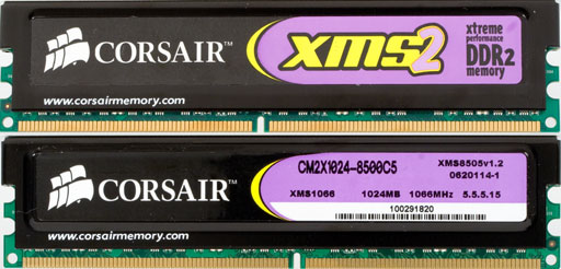 Module Part NumberModule Part Number Expansion The manufacturer's web site does not publish the DDR2 Part Number expansion of XMS2-series memory modules. TWIN2X1024-8500 Specs run that this product is a kit of two 1 GB modules, based on sixteen 64M x8 chips. These modules support the open standard EPP (SPD extension), developed by Corsair and NVIDIA. It allows to configure memory modules for maximum performance automatically on motherboards that support this standard. The manufacturer guarantees operation of these modules in DDR2-1066 mode with EPP 5-5-5-15-2T timings and 2.2 V voltage. But the default mode in the standard SPD section is the maximal standard DDR2-800 mode with 5-5-5-15 timings. SPD chip dataDescription of the general SPD standard:
Description of the specific SPD standard for DDR2:
Data of the "standard" SPD section are usual for Corsair modules. The fastest mode these modules are capable of is characterized by the cycle time of 2.5 ns (400 MHz, DDR2-800). This mode corresponds to the first supported value of tCL = 5, the full timing scheme is written as 5-5-5-18, which slightly disagrees with official characteristics, published in the datasheet on these modules (DDR2-800, 5-5-5-15). Reduced CAS# latency (CL X-1 = 4) corresponds to the non-standard cycle time of 3.7 ns, 270 MHz — it probably means DDR2-533 and the cycle time of 3.75 ns. Nevertheless, the incorrect cycle time results in fractional timings, which can be written (rounded to one figure after the dot) as 4-3.4-3.4-12.2, which will most likely be rounded up by most BIOS's to 4-4-4-13. In fact, DDR2-533 mode is evidently irrelevant for such fast modules, so these values hardly make any sense — it would have been better to remove them from SPD. Manufacturer’s JEDEC ID Code and Part Number of the module are correct. Nevertheless, as in the other Corsair modules, the SPD chip of these modules lacks information about the manufacturing date and serial number. Well, let's review the most important data from the "non-standard" SPD section that corresponds to EPP profiles, represented by Bytes 99-127. EPP Standard Description:
You can see that our modules support the EPP standard and contain information on two full profiles (or four abbreviated profiles that lack most latency and voltage tweaks for various signal lines). The first profile (Profile 0) corresponds to the 2.5ns cycle time, that is DDR2-800 mode. But unlike the standard SPD section, EPP Profile 0 specifies 4-4-4-12 for this mode, 2T address command rate and 2.0 V voltage, as well as other timing and voltage parameters that are not included into the table. The second EPP profile (Profile 1) is marked as optimal (recommended to be used by default), it corresponds to DDR2-1066 mode with the 1.875ns cycle time. Corresponding timings cannot be represented by integer values. It's written as 5-5.06-5.06-14.93, which must be read by motherboards with EPP support as 5-5-5-15. Address command rate in this case is also 2T, but the voltage is increased to 2.2 V. Testbed configurationsTestbed 1
Testbed 2
Testbed 3
Testbed 4
Test ResultsPerformance testsWe ran our tests on the ASUS M2N32-SLI Deluxe motherboard that supports EPP memory modules. EPP profiles can be enabled/disabled in BIOS Setup of this motherboard from the "SLI-Ready Memory" option, which can take the following values: "Disabled", "Optimal", "High Performance" and "High Frequency". "Disabled" evidently means using the standard memory settings from SPD. There are also "Optimal" (according to EPP data), "High Performance" and "High Frequency" profiles (these notions are rather wide, so the choice of a profile probably depends on your memory modules). In addition to the "SLI-Ready Memory" option we have "SLI-OC". It allows to overclock a processor by specified percent (from 0%, that is no overclocking, to 14% at 1% steps, plus the "MAX" option, which seems to correspond to 15% overclocking) to get maximum memory performance. The motherboard manufacturer warns that this mode may require increasing the CPU voltage, which is only natural. Along with these options, the ASUS M2N32-SLI Deluxe motherboard offers a great number of timing settings supported by the new DDR2 controller in AM2 processors (from standard tCL, tRCD, tRP, and tRAS to such insignificant settings as tRDRD/tWRWR), as well as various tweaks of latencies and voltages provided by the new EPP standard. Most of these parameters were set by default in our tests ("Auto"), that is we completely trusted automatic optimization of memory characteristics by EPP profiles. We tested these modules in four different ways: 1. SLI-Ready Memory: Disabled, it corresponds to the default SPD mode, that is DDR2-800, 5-5-5-18 timings, 2T address command rate 2. SLI-Ready Memory in "High Performance" mode, which also corresponds to DDR2-800, but with 4-4-4-12-2T latencies, EPP Profile 0. 3. SLI-Ready Memory in "Optimal" or "High Frequency" modes. It makes no difference in case of our modules, as the optimal EPP profile is set to Profile 1, which corresponds to maximum frequency. Interestingly, the motherboard operating in this mode reconfigured FSB clock and CPU multiplier so that its clock frequency remained on the previous level (2400 MHz = 240 MHz x10), but the memory frequency was increased from 400 MHz to 480 MHz (2400 /5). Timings are selected by Profile 1 — 5-5-5-15-2T. 4. The last test mode is similar to the previous one, but we allowed the motherboard to overclock the processor by setting "SLI-OC" to "MAX" (as we have already noted, it probably overclocks CPU by no more than 15%). We also increased the CPU voltage to 1.55 V, to make sure it worked well at the increased frequency. It ran at 2670 MHz (267 MHz x10) — this frequency is sufficient to raise the memory bus clock to approximately 533 MHz (2670 /5). Thus, the processor was overclocked by approximately 11%.
Test results in all the four modes are quite obvious. Differences between the first two modes, which differ only in timings, are less noticeable. Maximum real memory bandwidth is about 7.8-7.9 GB, which conforms well with the fact that even DDR2-800 memory (in dual-channel mode) is evidently excessive for single-core memory access from AMD AM2 processors. In conformity with this fact, memory bandwidth values demonstrated in the third mode (480 MHz memory, DDR2-960) are practically no different from the results demonstrated in the first two cases. Higher memory frequencies, while the CPU clock is preserved at 2.4 GHz, slightly reduce latencies, which is especially noticeable during random memory access. Only in the last case (Testbed 4), when we overclock the processor to 2.67 GHz (by 11%), maximum real memory bandwidth grows to about 9.0 GB/s, that is approximately by the same 11%. At the same time, we can see some latency reduction that has to do with lower absolute timings (5-5-5-15 at 533 MHz — lower than the same timing scheme at 480 MHz). Stability testsMemory timings, except for tCL, were adjusted "on the fly" with the built-in RMMA feature that allows to change dynamically memory settings, supported by the chipset (we used an intermediate version of this utility, RMMA 3.7, that already supports DD2 memory controller in AM2 processors.) Memory operating stability was evaluated with an auxiliary utility RightMark Memory Stability Test, included into RMMA.
Memory voltage in the first case was specified manually in compliance with the official recommendations, written in EPP profiles (2.0 V for DDR2-800). In all the other cases we left it up to the motherboard, which could configure system components automatically by EPP data. Minimal timings in the first two cases with 400 MHz memory were 4-4-3 at the reduced address command rate 1T (as always, tRAS values were not included into this scheme, as it could take any value, up to 5, without any effect on memory stability). These timings expectedly reduced latencies (compared to standard 4-4-4-12 and, especially, 5-5-5-18), but had practically no effect on memory bandwidth. In the third case, minimal stable timings for 480 MHz memory were 5-4-3 at the address command rate of 2T. Memory frequency increased to 533 MHz (Testbed 4) actually allowed to use the same timings, but errors occurred rather quickly. So the minimum possible timings in the native DDR2-1066 mode are 5-5-4 and the 2T address command rate. Nevertheless, "overclocking timings" had practically no effect on memory bandwidth (as in the first two cases) as well as on memory access latencies. Bottom lineCorsair XMS2-8500C5 proved to be high-performance high-end modules, which can operate in the official DDR2-800 mode as well as in the unofficial fastest DDR2-1066 mode (at the moderately high voltage of 2.2V). These modules, which SPD chips contain data of the new open EPP standard, are fully compatible with the ASUS M2N32-SLI Deluxe motherboard supporting this standard. Like the previously reviewed Corsair XMS2-8500, these modules offer moderate timing overclocking potential (compared to earlier top solutions from Corsair) — in the official DDR2-800 mode they can operate with 4-4-3-1T timings (2.0 V), the fastest DDR2-1066 mode requires increasing this scheme to 5-5-4-2T, still a tad lower than the recommended 5-5-5-2T scheme. Write a comment below. No registration needed!
|
Platform · Video · Multimedia · Mobile · Other || About us & Privacy policy · Twitter · Facebook Copyright © Byrds Research & Publishing, Ltd., 1997–2011. All rights reserved. | |||||||||||||||||||||||||||||||||||||||||||||||||||||||||||||||||||||||||||||||||||||||||||||||||||||||||||||||||||||||||||||||||||||||||||||||||||||||||||||||||||||||||||||||||||||||||||||||||||||||||||||||||||||||||||||||||||||||||||||||||||||||||||||||||||||||||||||||||||||||||||||||||||||||||||||||||||||||||||||||||||||||||||||||||||||||||||||||||||||||||||||||||||


