Major tasks for the nearest future of Intel's semiconductor technologies
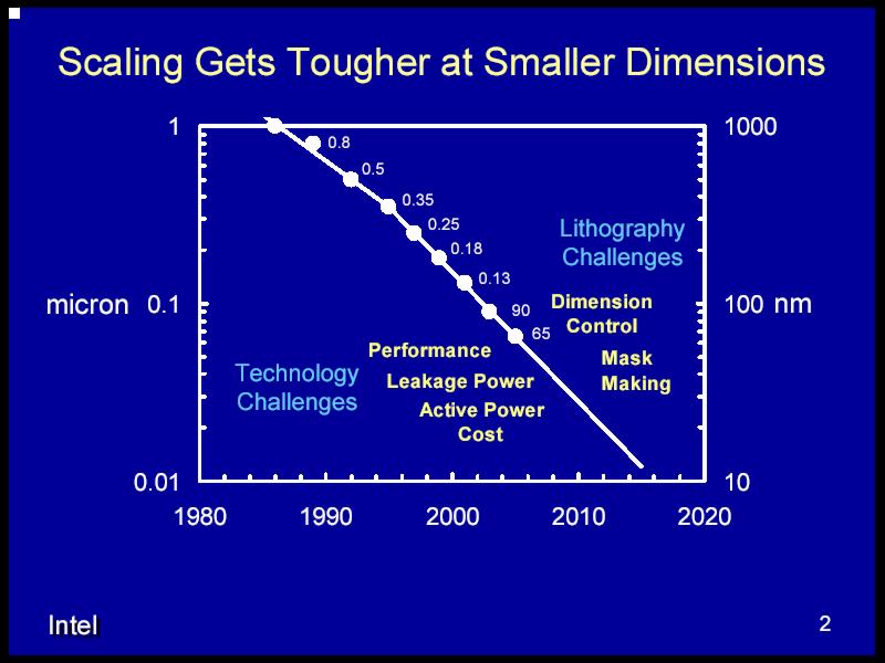
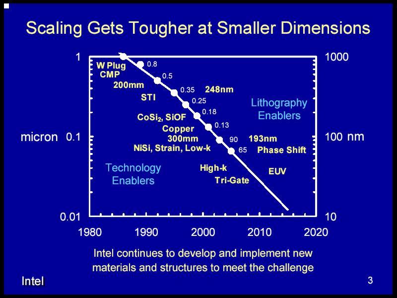
Having reviewed the 65nm process technology conceived by Intel corporation, let's proceed to a more general analysis of technological problems and tasks, which must be solved to realize this and subsequent, still "smaller" in terms of transistor dimensions, processes. It's not for nothing that the presentation of the 65nm process technology held at IDF 2004 Russia could have been opened with the slogan "Scaling gets tougher at smaller dimensions". Tasks and their solutions can be divided into two categories – technological and lithographic.
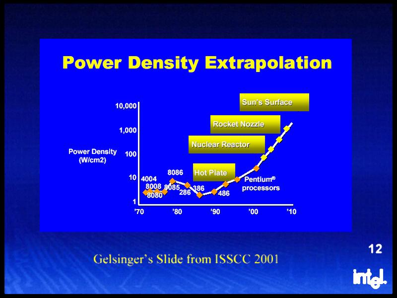
Technological tasks of the future semiconductor technologies from Intel and their solutions (on top). Increasing power density of microprocessors as the process technology progresses (below) is just an interesting analogy between hot plates, nuclear reactors, rocket nozzles, and Sun's surface, which the author found by chance in one of Intel's presentations...
Technological tasks
What are the major technological tasks of the future semiconductor technologies? Among the most important Intel notes the following: performance (obviously meaning the increasing difficulty of "frequency built-up" or "Gigahertz race" the company likes so much), the problem of leakage current reduction and the "costs" of further increase of effective output (increase of the ION / IOFF ratio).
Transistor dimensions
Problems
Solutions
90-65 nm
Performance
Strained silicon, nickel silicide
(NiSi), low-k dielectric (CDO) for interconnects
65-45 nm
Leakage current
high-k dielectric for a gate insulating
layer
45-30 nm
Effective output
Tri-gate transistors
On the table above you can see that the performance problem, which
is referred to 90-65nm process technologies, can be considered solved:
present and future microprocessors successfully use and will use silicon
"strain", nickel silicide for gate coating (as well as source-drains
coating), CDO dielectric with low-k to isolate copper interconnects
and reduce interconnect capacitance. In this connection, it'll be
more interesting to dwell on the second problem, which refers to not
so distant a future – leakage current problem. And let's defer
the problem of effective output and tri-gate transistor technology
for our future articles on this issue.
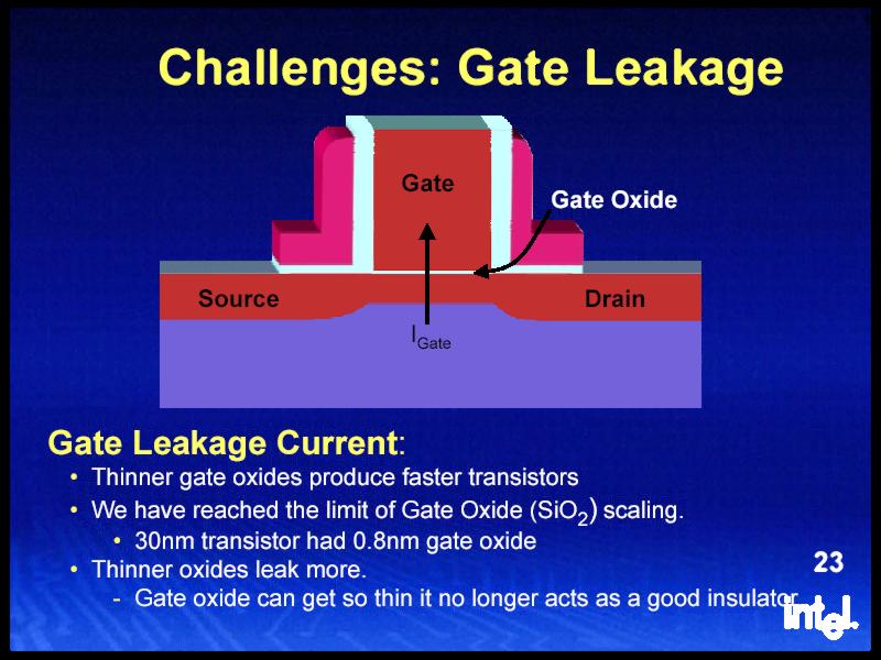
Problem of leakage current
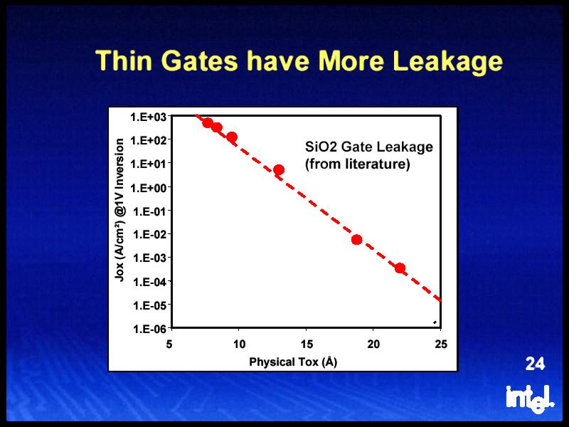
As we have already noted above in our analysis of the present 90nm and future 65nm process technology, silicon dioxide (SiO2) has been used as dielectric material for gates for 30 years already, mainly because its capacity to increase transistor performance by reducing the thickness of the insulating layer it forms. Nevertheless, further reduction of the oxide layer thickness (1.2 nm in 90nm and 65nm processes is only 5 atom layers!) is inevitably accompanied by undesirable effects. First of all, it's the increase of leakage current via the gate dielectric (IGate), which results in a considerable increase of power consumption and dissipation as well as "anomalous" transistor behaviour (note that these problems were the reason why the 90nm 4.0 GHz Pentium 4 Prescott processors had never come out and have been recently completely removed from the development program).
The problem of gate leakage current (IGate). On the left – explanation of the essence of the problem; on the right – dependence of leakage current on the gate oxide thickness.
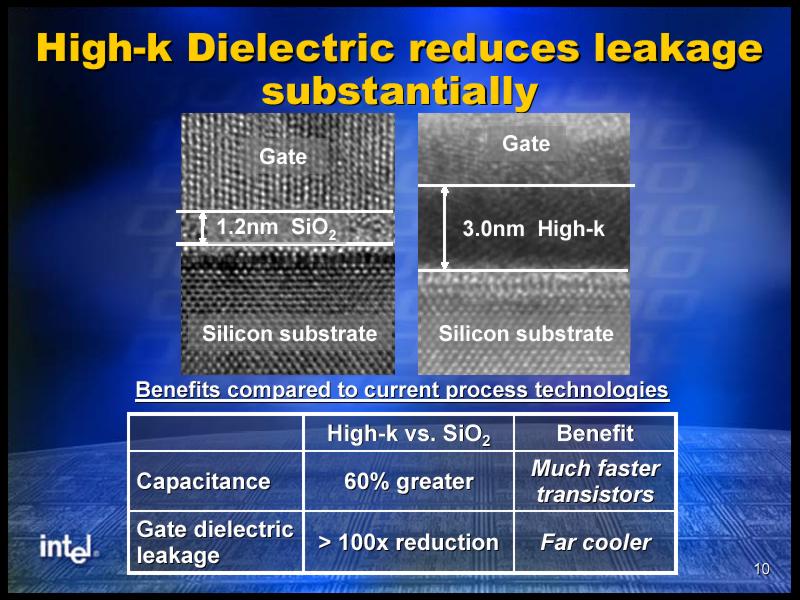
To solve this critical problem, Intel is planning to replace the current material of the gate dielectric (SiO2) with a thicker layer of the high-k material with better isolating properties, which creates high capacitance between the gate and the transistor channel (according to Intel, the "high-k" name derives from "high capacitance"). The first property of such material considerably reduces the leakage current, that is the "passive" power consumed by the transistor, while the second allows a considerably increased switching speed. Zirconium and hafnium oxides are noted in literature as preferable high-k materials.
High-k dielectrics as materials for a gate insulating layer.
Nevertheless, the use of high-k materials is presently significantly impeded by the problem of their "compatibility" with the electrode material – polycrystalline silicon (poly-Si). There appear two undesirable effects, when a high-k dielectric is combined with a polysilicon gate: Fermi level pinning and phonon scattering. The first effect is connected with some defects appearing on the border between the dielectric and the gate material and impeding the reduction of threshold voltage (i.e. the voltage level which switches the transistor state when applied to the gate), which is necessary to reach high transistor performance. The second effect is caused by the dielectric polarization, it reduces the mobility of charge carriers (electrons) and thus it also has a negative effect on the switching speed of transistors. To eliminate these undesirable effects, it's intended to use metallic gates (the choice of metal depends on the type of a transistor, PMOS or NMOS, and is currently not disclosed) and a special technique of transistor manufacturing. And finally, note that manufacturing such transistors as part of future Intel processors is expected in 2007 as an integral part of the 45nm process technology.