Intel notes the following lithographic challenges of the future: the problem of feature size control and mask techniques. Before we proceed to the brief overview of these problems and their solutions, let's dwell on the lithographic process in general.
Lithography means the process of creating necessary structural units
of a chip. As a rule, the current chip generation is composed of a
silicon substrate with over 20 layers of various materials on its
surface, which form structural units – transistors and feature
connectors ("wires"), which combination specifies necessary
configuration of the final product – be it a microprocessor,
chipset, memory, or any other chip type.
The lithographic process actively employs so called "masks". They are like a black-and-white negative, but only two gradations are used instead of shades of gray – full light transmission and full light absorption. The masks themselves are composed of a glass substrate with a dye "pattern" on it. The pattern is transferred from the mask to a silicon plate by projecting light of a certain wavelength through the mask.
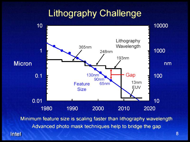
Lithography challenges for the nearest and distant future. The main problem is the increasing gap between the lithography wavelength and the decreasing feature size.
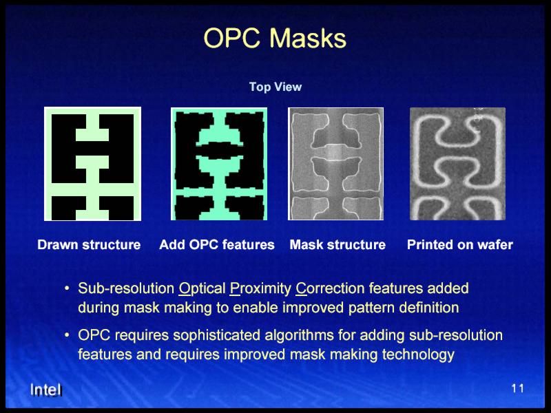
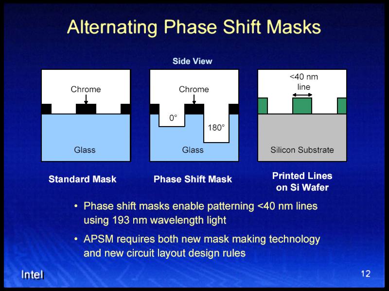
Development of the process technology as such obviously requires developing the lithography technique in use. The key element of the lithographic technique is the wavelength of the light source. Shorter-wave source allows smaller structural units, but this comes at the cost of the light source and optics as well as other system components. The present generation of Intel's chips is manufactured with an ultraviolet light source with the wavelength of 193nm, which allows minimum size of the structural unit of about 50nm (that is a gate length of a 90nm transistor). It's obvious that manufacturing 65nm transistors (with 35nm gate length, as was already mentioned above) requires either reduced wavelength of the light source or other tricks. These days Intel has taken up the second way by advancing alternative, more economically efficient technological tricks to increase pattern definition during the lithographic transfer of the mask pattern to the plate, which are called Alternating Phase-Shift Masks, APSM and Optical Proximity Correction, OPC. These technologies allow patterning substrates with the required minimum feature size, however they require significantly reworked mask making technology.
Lithographic solutions for the nearest future. Optical Proximity Correction and Alternating Phase-Shift Masks technologies in making and patterning masks.
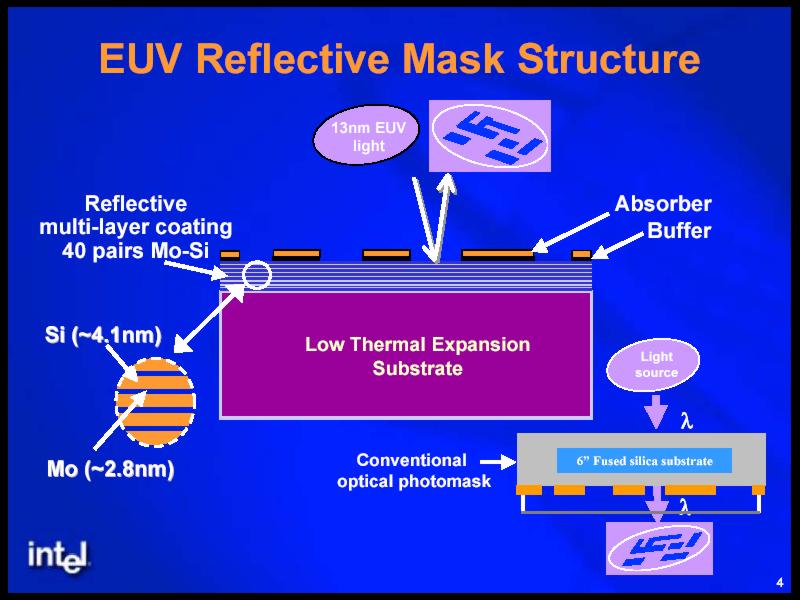
Nevertheless, the future process technologies will inevitably require a reduced wavelength of the emitter. Several presentations note the 157nm lithographic process as an intermediate solution. However, since the last IDF 2003 Russia, Intel has been planning the future lithographic techniques only as an introduction of the Extreme Ultra-Violet (EUV) technology with a huge wavelength leap of the light source far beyond the visible spectrum (which is within the 400-800nm wavelengths) into the far or hard ultra-violet radiation – to 13.5nm. While it's an obvious advantage from the point of view of resolution, a lot of technological problems are expected as well. The main problem is the absorption of such a short light by the lens material (quartz glass), which forces a fundamental technological reconstruction in the form of lens replacement with mirrors. In their turn, transmitting masks will have to be replaced with reflective ones (that is absorbing shortwave ultra-violet radiation in one spectrum and reflecting – in the other. Silicon molybdenum masks are planned to be used for this purpose). Besides, the entire plant must be put in absolute vacuum, because molecular nitrogen and oxygen also absorb well in this spectrum.
Lithographic techniques of the distant future. EUV lithography and reflective masks.
Conclusions
In fact, it's too early to make conclusions about the 65nm process technology, or moreover, about the future Intel technologies. As always, success or failure of the new technology will be demonstrated by ready solutions manufactured by this technology. And manufacturing 65nm processor cores is expected only next year. Besides, one can say that the process technology itself has not taken its final form yet. In our next articles we shall continue to review future semiconductor technologies, which are gradually becoming a part of the present. And there is nothing for us but to wait...