The nearest future of the semiconductor technologies from Intel: 65nm process technology
Having reviewed the current state of affairs in the industry, it'll be only logical to proceed to the new 65nm process technology, which has been already demonstrated in 70Mbit pilot samples of cache memory with 0.57 µm2 SRAM cells to be put into production in 2005. As always, we'll start with the key points, which are essentially similar to the 90nm process technology points we have just reviewed above. Nevertheless, it's important to note that the information below is of somewhat "preliminary" character, because more information on Intel's 65nm logic technology will be presented in about 1.5 months at the IEEE International Electron Devices Meeting in San Francisco Dec. 12-15 2004.
1. Improved strained silicon technology
Strained silicon technology, which Intel has used starting from the 90nm process technology reviewed above, gets its further development in the 65nm process technology. Enhanced strained silicon technology provides the new process technology with still higher switching speed of the transistors due to increased by 10-15% drive current (ID, or ION) at practically constant leakage current via the gate oxide layer (IGate). According to Intel, the advanced silicon strain technology of the second generation will raise the clock frequency by 30% (in comparison with "non-strain" silicon).
2. New 65nm transistors
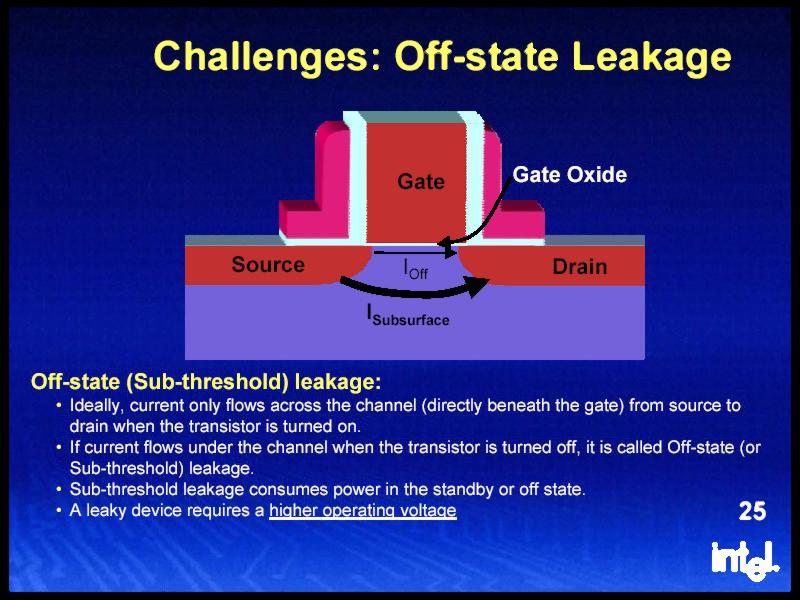
65nm transistors are characterized by further reduced nickel silicicated polysilicon gate length to 35 nm at the retained gate oxide thickness of 1.2nm. The latter factor helps preserve the leakage current at the same level, and the combination of these factors reduces gate capacitance (CGate) to 20%, which reduces chip active power. Nevertheless, we shouldn't forget about such an important characteristic of a field transistor as off-state current (IOFF) – the current flowing from the source junction to the drain junction of the transistor when it is turned off, which is induced by partial breakdown of the gate material as well as of the wafer material. The newest presentation of the 65nm process technology makes no mentions of this fundamental issue. To be more exact, IOFF is to all appearances subtly substituted for IGate! But it's well known from literature that the reduction of gate length will inevitably increase IOFF, which is not denied by Intel in several other presentations, by the way.
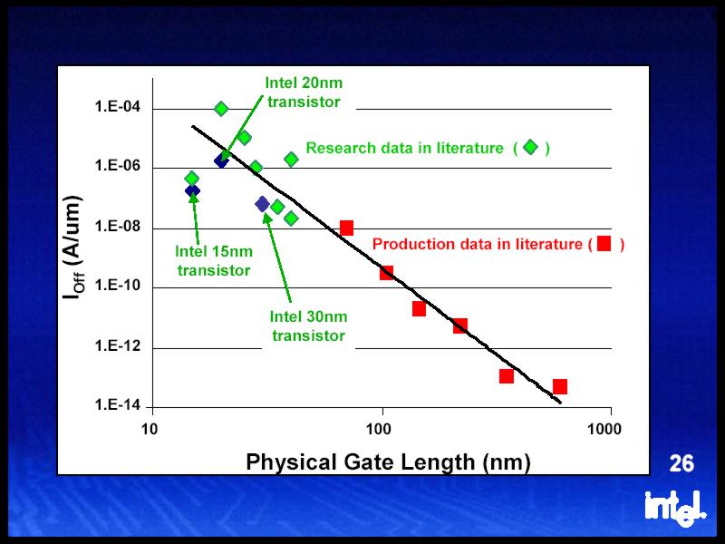
The problem of current leakage in off mode (IOFF). On top – explanation on the essence of the problem. Below – ION / IOFF ratio for 90nm and 65nm transistors according to the latest presentation of the 65nm process technology (on the left) and the dependence of IOFF on the gate length according to the presentation of "future transistors" from Intel (on the right). There are obvious IOFF inconsistencies between two different presentations from the same company.
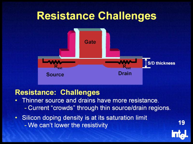
Out of additional new features implemented in 65nm transistors, first of all we should note their voltage reduced to 1.0 V, which has a positive effect on the dissipated power. What concerns materials, the new process technology completely switched to nickel silicide (NiSi) as a common material both for transistor gate coating as well as source and drain coating, which results in reduced electrical resistance of the latter and to additional reduction of power consumption. At last, the contacted gate pitch in the new process technology is reduced to 220 nm for higher density of chip elements.
The problem of increased source-drain material resistance at smaller dimensions. Solution to the problem in the 65nm process technology – nickel silicide (NiSi) used for coating these transistor components as well as for gate coating.
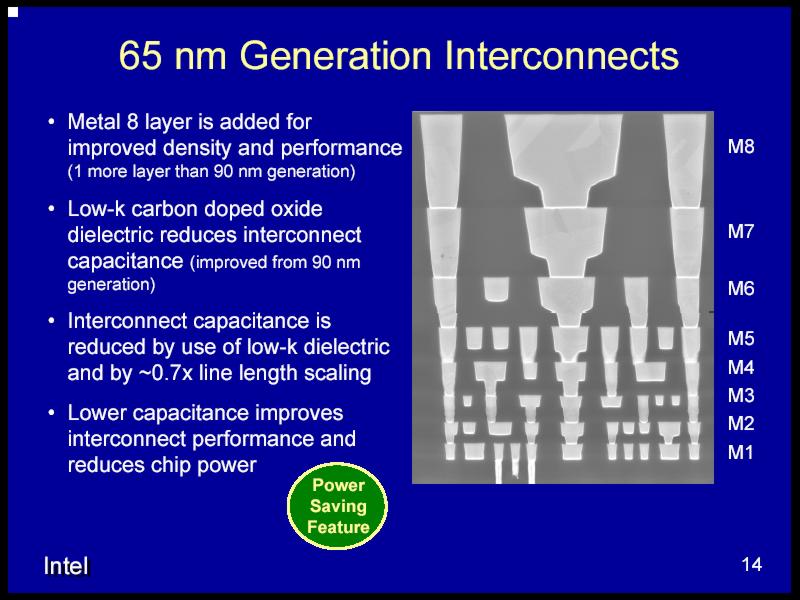
3. 8-layer transistor interconnects
The new process technology also introduces changes into the interconnect manufacturing scheme. First of all, another (the 8th) metal (copper) layer is added for improved density of contacts and higher propagation speed of electric signals. Low-k carbon doped (CDO) oxide is still used as dielectric, but its manufacturing technology is noted to be improved from 90nm generation. This new material together with the new method of 0.7x line length scaling of copper interconnects result in further reduction of interconnect capacitance, which leads to reduced chip power dissipated at transistor interconnects, as already noted in the previous chapter.
65nm transistor interconnects. General view and brief description of their manufacturing technique.
4. 0.57µm2 SRAM cells, sleep transistors
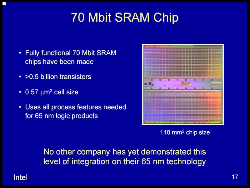
65nm process technology in manufacturing 4 Mbit SRAM chips was first announced by Intel in November 2003. Later on, the company managed to produce fully functional 70 Mbit SRAM chips by this process technology, which had a comparatively small die area – 110 mm2. Manufacturing SRAM chips with small area and high capacity is obviously essential to integrate large volumes of cache memory into a processor core, which in most cases has a positive effect on performance of the final product in real applications.
65nm SRAM chips. On the left – view of the chip and its specification; on the right – power saving properties of the chip due to sleep transistors
65nm SRAM chip cell packs six transistors (6T technology) in an area of 0.57 µm2 (for comparison, the area of a 6T cell in 90nm SRAM cache is 1.0 µm2) and is characterized by a relatively low static noise margin (SNM), which allows to operate at voltages of up to 0.7 V.
As is noted in the presentation of the 65nm process technology, an important distinction of the new 65nm SRAM chips is the usage of so called sleep transistors, which control the current flow to SRAM Cache sub-blocks depending on their state (sleep transistors shut off leakage in inactive sub-blocks, and cut it in when any of the elements of the array is accessed). The use of sleep transistors obviously results in considerable SRAM cache leakage reduction, which is especially important for mobile devices. Though this technology is considered a distinctive feature of 65nm SRAM devices, we should note that a similar (we do not contend that it's the same) technology has been actually implemented and used since 130nm Pentium M mobile processors with Banias core, capable of putting to sleep inactive parts of L2 cache.
5. 300 mm wafer fabs
65nm chip production involves the same 300mm wafers that are used in manufacturing the current generation of 90nm processor cores. Pilot production of 65nm devices is currently running in D1D fab in Hillsboro, Oregon, where this process had been developed.