 |
||
|
||
| ||
|
||
|
||
| ||
Nobody is lost? Here we're entering the second server room: It is relatively empty. Right in front of you is a line prepared for units of computational servers. On the right is a young growing cluster processing tasks for NV50: 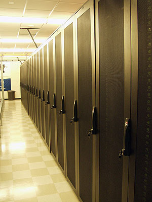 Not all of these cases are filled. For example, the one below has only a carefully prepared screwdriver: 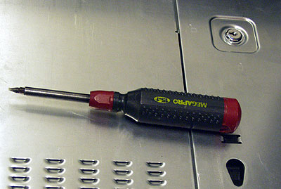 These mounts and servers have several advantages over those in the old building, that is why they are chosen for further development. 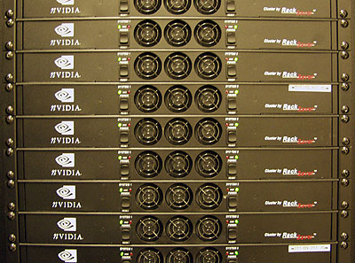 Each unit contains two (!) dual-processor boards for Pentium 4 (Xeon DP), i.e. from 2 to 4 processors in one case which is also thinner than that of the old cluster. In future HT processors can also be installed. Their back looks not less impressive: 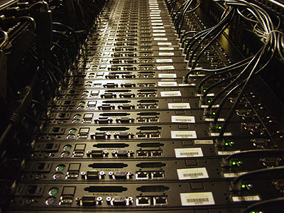 The cooling system is arranged in an interested way - warm air is blown out of the server sides and then goes up along special channels. Around 3000 processors are already installed and others keep on arriving (5000 more are expected). Well, NVIDIA is raising new forces for the oncoming attack on the graphics market... Results obtained must be reliably saved. Fur this purpose they have intellectual SAN units with quickly replaceable storage devices (Avaya) 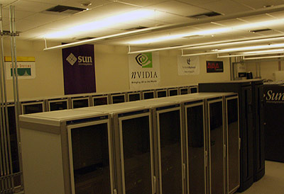 Configurable and controlled by a special touch-screen server, 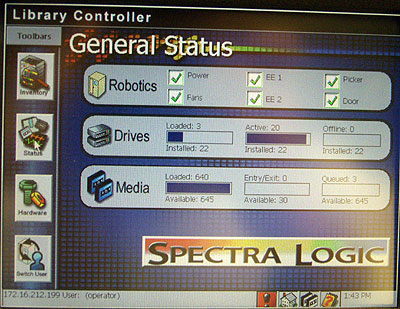 the storage devices are optically interconnected and connected with the servers; tasks of the utmost importance are used on a special system built on Sun Stor Edge 9900, a very efficient expensive file server with its own controller. 5 minutes to look for those who got lost among the rows of servers and storage units, and then we will move on to the next door which contains strategic stocks of spare parts: 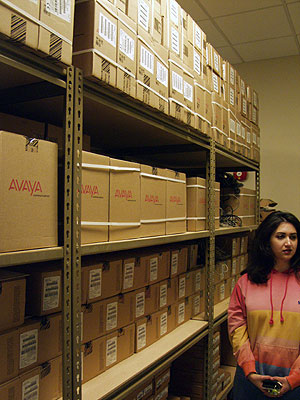 storage devices, mainboards, processors etc. Before we go to the cafe let's drop in one more interesting place often neglected for some reason 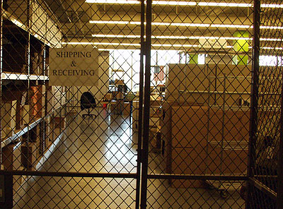 Shipping and receiving... reminds a department of a classic American post office. Chips come here and leave this place, as well as other various devices necessary for the company's functioning. They tell jokes... how, at the dawn of the company one of its future vice-presidents did his job in the day time and helped to test and pack chips in the evening :-) Will you please hold for me a box of NV30 chips for a couple of months? :-)  Now let's have a snack at what NVIDIA calls nth Street Cafe  This cafe calls up memories about communism with its conception of distribution, abundance of people (especially during the dinner time) 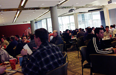 and very low prices especially for the USA. You can have a substantial meal at $6 choosing among Japanese and Chinese cuisine, healthy European salads, Italian pizzas and American junk food (hamburgers and stakes). To everyone's taste! After that you can have a game of mini football or table tennis with your colleagues: 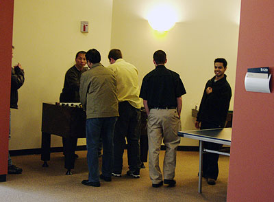 But I prefer to got to the laboratory of surgical tortures and vivisection of chips! If you remember, some time ago Russian chipmakers used to steal ideas and principles of the progressive foreign microprocessing solutions by sawing off layer by layer from dies and copying the topology. If I'm not mistaken, the last processor they could strip off was early 386 which failed to get into mass production and was used mostly for defense needs. Allegedly, they stopped copying because of too fine technological norms. But it's just a myth! It ceased due to some other reasons, probably, political or economical, but now NVIDIA has one of the most advanced laboratories for stripping.. layers from chips. It's not because NVIDIA gets extra orders for developing Intel processors for AMD :-), and not because NVIDIA tried to peep at something new in ATI's chips. It's simple - NVIDIA has to scour layer by layer (note that mechanical processing can be rarely used, but good concentrated acid solutions allow separating layers of even .13-micron chips) their own solutions. For debugging. Imagine that the first trial lot has arrived from TMSC factory - NV35 chips of revision 1. First they will be gripped in a special connector: 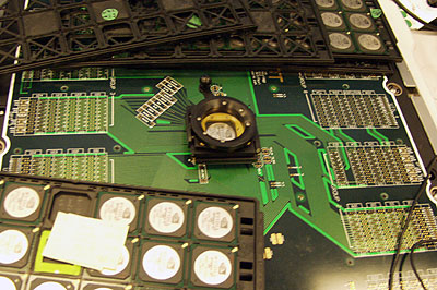 and then it will be checked whether all outputs are connected the right way, and the chip's internal diagnostics will be done through a special built-in debug port. 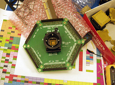 Here you can see one more connector and a chip pinout map - different group of pins are marked with different colors. Imagine, everything looks operable, or at least, most part of the interface functions work. Let's connect the chip to the computer and oscillographs to test it thoroughly: 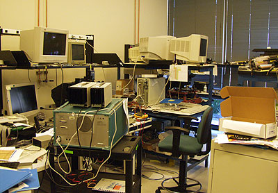 But sometimes it can be a real problem to find out why a chip may not start - even simplest functions and debugging can fail to work. Then it should be disassembled and examined 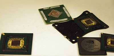 First, it's necessary to check whether all pins are connected as supposed: 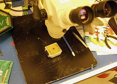 and it has any mechanical damage or artifacts (wrong packaging). If it's Ok, the problem can be in the chip itself. What should we do? It worked perfectly at the emulation stage, and now crops up a defect. Is it a production defect or it's caused by the wrong chip's layout? Maybe, the template has a flaw? This is when it's necessary to scour the chip layer by layer and examine it with an electronic microscope. But it's not that simple - it's necessary to develop a new technique for different types of packages and dies especially if the technology changes. Patricia is a chief experts in these matters at NVIDIA. She jokes that she seems to be the only native (born in America) scientist with the company :-) Patricia, what's there lying in the corner? Isn't it symbolic: 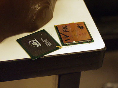 So, the technology of scouring 0.13 micron chips was needed long before first NV30s. The first of the available experimental samples is on the table :-): 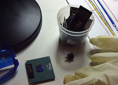 Right you are - this is Intel Pentium III. It has a lot of useful stuff next to it: bolts, keys, cones and chips: 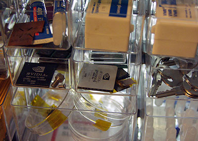 [ Third Page ]
Alexander Medvedev (unclesam@ixbt.com)
Write a comment below. No registration needed!
|
Platform · Video · Multimedia · Mobile · Other || About us & Privacy policy · Twitter · Facebook Copyright © Byrds Research & Publishing, Ltd., 1997–2011. All rights reserved. |


