 |
||
|
||
| ||
And this is a glass of failures - when chips are disassembled and cleaned they can be damaged: 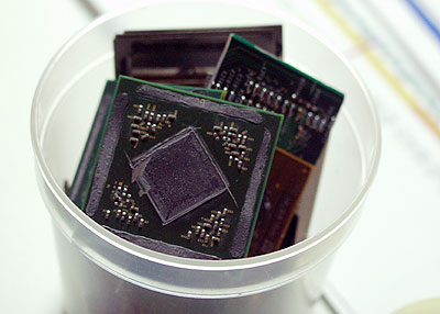 (this is the package with a flip die - remains of NV30). This kind of work requires huge experience and knowledge of chemistry and science of materials, as well as assiduity and laboriousness. A midget mistake, and the work comes to nothing. The red mash you can see below is actually a print-out topology of a small zone of one of the chip layers:  In the lab corner is a small chemical table where they carefully and accurately scour layers with acids (this machine measures out the reagents):  An emergency shower is located nearby: such acids can be very dangerous because even metals and silicon can suffer not to mention biological materials. Finally, we have disassembled the case and successfully defined the parameters having scoured all needed layers. How beautiful NVIDIA's baby NV31 looks with the upper layer taken away (see the beginning of the article)! The disassembled chip is placed under a powerful scanning tunnel microscope:  This device can show particles of even units of a nanometer. Having scanned the required area of the chip we can define many defects and examine the topology. This combined device can ascertain a composition of the substance around the chosen area! A defect can be caused by a foreign formation which might get there while the die chip was growing or assembled - and this gadget can determine the nature of such defect. Imagine there is an unwanted connection or break to be eliminated. Here is our plan of actions:  This gun emitting a focused ion ray will help fulfill cutting or welding of microscopic tracks in the respective chip's layer: 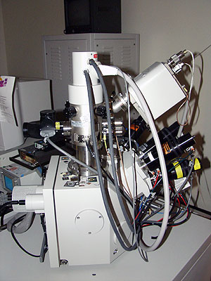 The chip corrected this way is not scoured and can be used for further testing and debugging. The possibility to correct a great number of errors at one pass saves a lot of money for the company - every new startup, new correction in templates and simply new chips require huge expenses. Thus, the laboratory of chips disassembling and surgery is not a redundant place for the company. So, the chip is debugged, and the second revision works stably. It's time to make cards, develop drivers and test for compatibility. The tests have to be carried out in different configurations and in different programs. Here is a variety of platforms for low-level tests:  Here are some more: 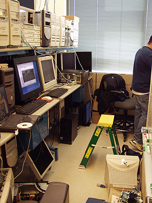 And here they have:  ...about 30 PC cases. They have a lot of such office rooms. Now have a look at the program testing drivers and some hardware for correct execution of various DirectX and GDI functions: 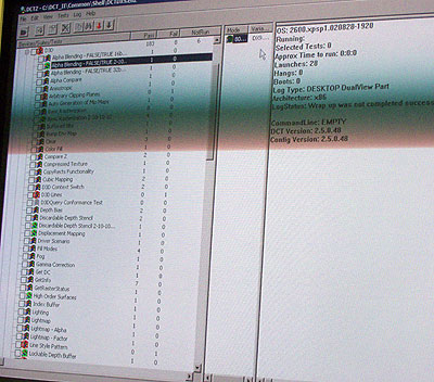 The test list is lengthy. Before handing in drivers to Microsoft for certification it's better to do it locally because certification is long and expensive, like chip production. For NV30 benchmarking they use cards with moderate rather quiet cooling (like on professional solutions):  Cards working improperly are revealed at the stage of driver and hardware compatibility testing. There is a whole box of such bad samples accumulated during the company's life:  The box is not that big as the testers actually receive operable samples already. The question is in compliance with programs and drivers. Below is NV3 (Riva 128) which is one of the first cards based on one of the first chip revisions. By the way, it successfully traversed the Pacific as a NVIDIA's contribution to our hardware museum. They said it worked pretty well though some slight bugs were still there:  Now we are moving to the benchmarking section which contains a plenty of various configurations for performance comparison. Intel's solutions and latest RADEONs (in the button left-hand corner) are not ignored either: 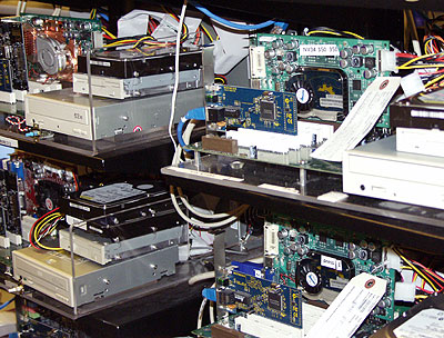 Well, it's necessary to keep an eye on the competitors, be aware of their weak and strong points. Besides, it's also necessary to watch reviewers - what if they get odd results - here they can check whether a fatal error has crept in. Moreover, performance of their own drivers has to be tracked as well. What's this?  Here it is. The clock speeds are equal to NV31, but the chip is NV34. The chip has reserve in the core clock speed and is pin-compatible with NV31, that is why the common reference design can be used. Look at NV31 (this was the first card I saw "alive"): 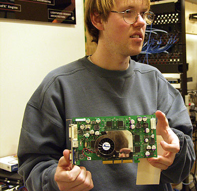 It does work and it run applications. You can look through 3D Marks (2001). This is a corner of really creative people - some of them think out chips, others make advertising and PR materials. Some fill up the boards with schemes of anisotropy and formulas in a burst of creativity:  Some decorate their rooms with photos of children and darlings:  Other have pictures of well-known virtual heroes: 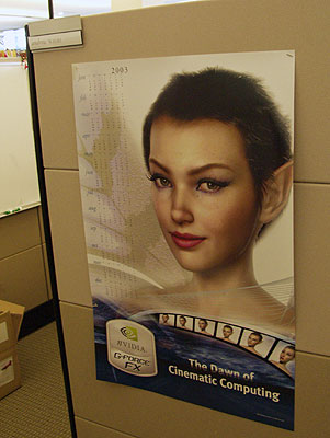 Somewhere research labs won't let you pass without a PocketPC (thankfully, I got one):  Here one can play my favorite game - basketball:  Are you tired? The very last place I'm going to call in is NVIDIA's museum which would be more interesting for the investors and mass media. It's decorated very attractively: 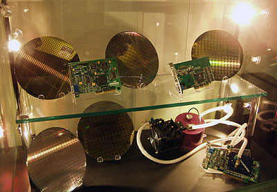 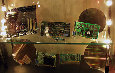 It houses everything from NV1 to NV30. Next to it is a passage with patents hanging on the walls:  Isn't it beautiful? They have heaps of them. That's all. However, I don't think this was the last excursion. In half a year or so I will try to get there again to find more interesting worthy things. Good bye! And it was nice to meet you!
Alexander Medvedev (unclesam@ixbt.com)
Write a comment below. No registration needed!
|
Platform · Video · Multimedia · Mobile · Other || About us & Privacy policy · Twitter · Facebook Copyright © Byrds Research & Publishing, Ltd., 1997–2011. All rights reserved. |