NVIDIA GeForce 6800 Ultra (NV40). Part One: Architecture Features and Synthetic Tests in D3D RightMark
|
We've been waiting for it.
And finally, here is the new architecture:
a correction of past mistakes
and a solid foundation
for the future. But is it really so?
We are going to probe into both aspects.
CONTENTS
- Official specs
- Architecture
- 2D and the GPU
- Videocard features
- Synthetic tests in D3D RightMark
- Quality of trilinear filtering and anisotropy
- Conclusions
The article is mainly devoted to issues of architecture and synthetic
limiting tests. In a while, an article on performance and quality
of game applications will appear, and then, after a new ATI architecture
has been announced, we'll conduct and publish a detailed comparative
research of quality and speed issues of AA and anisotropic filtering
in the new-generation accelerators. Before reading this article make
sure you have thoroughly studied
DX Current and DX Next, materials
on various aspects of today's hardware graphic accelerators, and on
architectural features of NVIDIA and ATI products, in particular.
GeForce 6800 official specs
- Chip codenamed NV40
- 130nm FSG (IBM) technology
- 222 million transistors
- FC case (flip chip with no metallic cover)
- 256-bit memory interface
- Up to 1 GB of DDR / GDDR -2/ GDDR -3 memory
- Bus interface AGP 3.0 8x
- A special APG 16x mode (both ways), for PCI Express of HSI bridge
- 16 pixel processors, each having a texture unit with an optional filtering of integer and float-point textures (anisotropy up to 16x).
- 6 vertex processors, each having one texture unit with no value filtration (discrete selection)
- Calculates, blends, and writes up to 16 full pixels (colour, depth, stencil buffer) per clock
- Calculates and writes up to 32 values of depth and stencil buffer per clock (if no operation with colour is executed)
- Supports a two-way stencil buffer
- Supports special optimisations of geometry rendering for acceleration of shadow algorithms based on the stencil buffer (the so-called Ultra Shadow II technology)
- Supports pixel and vertex shaders 3.0, including dynamic branchings in pixel and vertex processors, texture value selection from vertex processors, etc.
- Texture filtering in the floating-point format
- Supports framebuffer in the floating-point format (including blending operations)
- MRT (Multiple Render Targets - rendering into several buffers)
- 2x RAMDAC 400 MHz
- 2x DVI interfaces (require external chips)
- TV-Out and TV-In interface (requires separate chips)
- Programmable streaming GPU (for video compression, decompression and post-processing)
- 2D accelerator supporting all GDI+ functions
GeForce 6800 Ultra reference card specs
- 400 MHz core frequency
- 1.1 GHz (2*550 MHz) effective memory frequency
- GDDR-3 memory type
- 256-MB memory size
- 35.2 GBps memory bandwidth
- Theoretical filling speed: 6.4 Gpps
- Theoretical texture selection speed: 6.4 Gtps
- 2 DVI-I connectors
- TV-Out
- Up to 120 W energy consumption (the card has two additional power connectors, the power sources are recommended to be no less than 480 W)
General scheme of the chip
At the current detalisation level, no significant architectural differences from the previous generation are seen. And it is no surprise, as the scheme has survived several generations and is optimal in many aspects. We would like to note that there are six vertex processors and four separate pixel processors each working with one quad (a 2x2 pixel fragment). Also noteworthy are two levels of these textures' caching (a general cache and a personal cache for each group of 4 TMUs in the pixel processor), and, as a result, the new ratio of 16 TMUs per 16 pixels.
And now we'll increase detalisation in the most interesting places:
Vertex processors and data selection
An interesting innovation has been introduced: a support of various scalers for the flows of the vertices' source data. Let us remind you how data are generally selected for the vertices in modern accelerators:
The structure consists of several predefined parameteres: scalars and vectors up to 4D, floating-point or integer formats, including such special data types as vertex coordinates or normal vector, colour value, texture coordinates, etc. Interestingly, they can only be called "special" from the point of view of API, as hardware itself allows an optional parameter commutation in the microcode of the vertex shader. But the programmer needs to specify the source registers of the vertex processor, where these data will be after selection, in order not to make redundant data moves in the shader.
Vertex data stored in the memory must not necessarily be a single fragment, they can be divided into a number of flows (up to 16 in NV40) each having one or several parameters. Some of the flows may be in the AGP address range (that is, will be selected from the system memory), other may be placed in the local memory of the accelerator. Such approach allows to use twice the same data sets for different objects. For instance, we can separate geometrical and textural information into different flows, and having one geometrical model use different sets of textural coordinates and other surface parameters, thus ensuring an external difference. Besides, we can use a separate flow only for the parameters that have really changed. Others can be loaded just once into the local memory of the accelerator. A current index, single for all flows, is used to access the parameters of this or that vertex. This index either changes in a chaotic way (source data are represented as an index buffer) or gradually increases (separate triangles, stripes and fans).
What is new about the vertex data selection in NV40 is that it's not necessary for all the flows to have the same number of data sets. Each flow can have its own index value divider (a so-called Frequency Stream Divider). Thus, we avoid data duplication in some cases and save some size and bandwidth of the local memory and the system memory addressed through AGP:
Apart from that, the flow can now be represented as a buffer smaller in size than the maximal index value (even including the divider), and the index will just turn round the flow's buffer border. This novelty can be applied for many operations, for instance, to compress geometry using hierarchic representations or to copy features onto the array of objects (information common for each tree in the forest is only stored once, etc.).
And now take a look at the schematic of the NV40 vertex processor:
The processor itself is represented as a yellow bar, and the blocks surrounding it are only shown to make the picture more complete. NV40 is announced to have six independent processors (multiply the yellow bar by six) each executing its own instructions and having its own control logic. That is, separate processors can simultaneously execute different condition branches on different vertices. Per one clock, an NV40 vertex processor is able to execute one vector operation (up to four FP32 components), one scalar FP32 operation, and make one access to the texture. It supports integer and float-point texture formats and mipmapping. Up to four different textures can be used in one vertex shader, but there's no filtering as only the simplest access (a discrete one) to the nearest value by specified coordinates is possible. This enabled a considerable simplification of the TMU and consequently, of the whole vertex processor (the simpler the TMU - the shorter the pipeline - the fewer transistors). In case of urgency, you can execute filtering in the shader yourself. But of course, it will require several texture value selections and further calculations, and as a result, it will take many more clocks. There are no rigid restrictions as to the length of the shader's microcord: it is selected from the local memory of the accelerator during execution. But some specific APIs (namely, DX) may impose such restrictions. Given below is a summary table of the NV40 vertex processor's parameters concerning DX9 vertex shaders, compared to families R3XX and NV3X:
| Vertex shader version |
2.0 (R 3 XX) |
2. a (NV 3 X) |
3.0 (NV40) |
| Number of instructions in the shader
code |
256 |
256 |
512 and more |
| Number of executed instructions |
65535 |
65535 |
65535 and more |
| Predicates |
No |
Yes |
Yes |
| Temporary registers |
12 |
13 |
32 |
| Constant registers |
256 and more |
256 and more |
256 and more |
| Static jumps |
Yes |
Yes |
Yes |
| Dynamic jumps |
No |
Yes |
Yes |
| Nesting depth of dynamic jumps |
No |
24 |
24 |
| Texture value selection |
No |
No |
Yes (4) |
In fact, if we look back on the NV3X architecture, it becomes clear that NVIDIA developers only had to increase the number of temporary registers and add a TMU module. Well, now we are going to see synthetic test results and find out how close NV40 and NV3X architectures are in terms of performance.
And another interesting aspect we will dwell on is performance of the FFP emulation (of the fixed T&L). We would like to know if NV40 hardware still has the special units that gave NV3X such a visible increase on the FFP geometry.
Pixel processors and filling organisation
Let's examine the NV40 pixel architecture in the order of data sequence. So, this is what comes after the triangle parameters are set:
Now we are going to touch upon the most interesting facts. First, in contrast
to earlier NV3Xs that only had one quad processor taking a block of
four pixels (2x2) per clock, we now have four such processors. They
are absolutely independent of one another, and each of them can be
excluded from work (for instance, to create a lighter chip version
with three processors in case of them has a defect). Then, each processor
still has its own quad round queue (see DX
Curent). Consequently, they also execute pixel shaders similarly
to the way it's done in NV3X: more than a hundred quads are run through
one setting (operation) followed by a setting change according to
the shader code. But there are major differences too. First of all,
it concerns the number of TMUs: now we only have one TMU per each
quad pixel. And as we have 4 quad processors with 4 TMUs in each,
it makes the total of 16 TMUs.
The new TMUs support anisotropic filtering with the maximal ratio of 16:1 (the so-called 16x, against 8x in NV3X). And they are they first to be able to execute all kinds of filtering with floating-point texture formats. Although, providing the components have a 16-bit precision (FP16). As for FP32, filtering still remains impossible. But the fact that the FP16 level has been reached is already visible progress. From now on, floating-point textures will be a viable alternative to integer ones in any applications. Especially as FP16 textures are filtered with no speed degradation. (However, an increased data flow may and probably will impact on performance of real applications.)
Also noteworthy is a two-level texture caching: each quad processor has its own first-level texture cache. It is necessary to have one for two following reasons: the number of quads processed simultaneously has increased fourfold (quad queues haven't become longer, but the number of processors has risen to four), and there is another access to the texture cache from vertex processors.
A pixel has two ALUs each capable of executing two different operations on different numbers of randomly selected vector components (up to four). Thus, the following schemes are possible: 4, 1+1, 2+1, 3+1 (as in R3XX), and also the new 2+2 configuration, not possible before (see article DX Current for details). Optional masking and post-operational component replacements are supported too. Besides, ALUs can normalise a vector in one operation, which can have a considerable influence on performance of some algorithms. Hardware calculation of SIN and COS values was extracted from the new NVIDIA architecture: it was proved that transistors used for these operations were spent in vain. All the same, better results in terms of speed can be achieved when accessing by an elementary table (1D texture), especailly considering that ATI doesn't support the mentioned operations.
Thus, depending on the code, from one to four different FP32 operations on scalars and vectors can be made per clock. As you can see in the schematic, the first ALU is used for service operations during texture value selection. So, within one clock we can either select one texture value and use the second ALU for one or two operations, or to use both ALUs if we're not selecting any texture. Performance is directly related to the compiler and the code, but we definitely have the following variants:
Minimum: one texture selection per clock
Minimum: two operations per clock without texture selection
Maximum: four operations per clock without texture selection
Maximum: one texture selection and two operations per clock
According to certain information, the number of temporary registers for quad has been doubled, so now we have four temporary FP32 registers per pixel or eight temporary FP16 registers. This fact must incerase dramatically performance of complex shaders. Moreover, all hardware restrictions as to the pixel shaders' size and the number of texture selections have been removed, and now everything depends on API only. The most important modification is that execution can now be controlled dynamically. Later, when the new SDK and the next DirectX 9 (9.0c) version appear, we'll conduct a thorough study of realisation and performance of pixel shaders 3.0 and dynamic branches. And now take a look at a summary table of capabilities:
| Pixel shader version |
2.0 (R3XX) |
2.a (NV3X) |
2.b (R420?) |
3.0 (NV40) |
| Bëoæehhoctü texture selections, maximum |
4 |
No restrictions |
4 |
No restrictions |
| Texture value selections, maximum
|
32 |
No restrictions |
No restrictions |
No restrictions |
| Shader code length |
32 + 64 |
512 |
512 |
512 and more |
| Number of shader instructions executed
|
32 + 64 |
512 |
512 |
65535 and more |
| Interpolators |
2 + 8 |
2 + 8 |
2 + 8 |
10 |
| Predicates |
no |
yes |
no |
yes |
| Temporary registers |
12 |
22 |
32 |
32 |
| Constant registers |
32 |
32 |
32 |
224 |
| Optional component rearrangement |
no |
yes |
no |
yes |
| Gradient instructions (D D X/ D DY)
|
no |
yes |
no |
yes |
| Nesting depth of dynamic jumps |
no |
no |
no |
24 |
Evidently, the soon-to-be-announced ATI (R420) architecture will support the 2.b profile present in the shader compiler. Not willing to make hasty conclusions, we'll say however, that NV40's flexibility and programming capabilities are beyond comparison.
And now let's go back to our schematic and look at its lower part. It contains a unit responsible for comparison and modification of colour values, transparency, depth, and stencil buffer. All in all, we have 16 such units. Considering the fact that comparison and modification task is executed quite similarly in every case, we can use this unit in two following modes.
Standard mode (executes per one clock):
- Comparison and modification of depth value
- Comparison and modification of stencil buffer value
- Comparison and modification of transparency and colour component values (blending)
Turbo mode (executes per one clock):
- Comparison and modification of two depth values
- Comparison and modification of two stencil buffer values
Certainly, the latter mode is only possible if there's no calculated and writable colour value. That is why the specs say that in case there's no colour, the chip can fill 32 pixels per clock, estimating the values of depth and stencil buffer. Such turbo mode is mainly useful for a quicker shadow building basing on the stencil buffer (the algorithm from Doom III) and for a preliminary rendering pass that only estimates the Z buffer. (Such technique often allows to save time on long shaders as overlap factor will be reduced to one).
Luckily, the NV3X family now supports MRT (Multiple Render Targets - rendering into several buffers), that is, up to four different colour values can be calculated and written in one pixel shader and then placed into different buffers (of the same size). The fact that NV3X had no such function used to play into the hands of R3XX, but now NV40 has turned the tables. It is also different from the previous generations in an intensive support of floating-point arithmetics. All comparison, blending and colour-writing operations can now be made in the FP16 format. So we finally have a full (orthogonal) support of operations with a 16-bit floating point both for texture filtering and selection and stencil buffer handling. Well, FP32 is next, but that will be an issue for the future generation.
Another interesting fact is the MSAA support. Like its NV 2X and NV 3X predecessors, NV40 can execute 2x MSAA with no speed degradation (two depth values per pixel are generated and compared), and it takes one penalty clock to execute 4x MSAA. (In practice, however, there's no need to calculate all four values within one clock, as a limited memory bandwidth will make it difficult to write so much information per clock into the depth and frame buffers). More than 4x MSAA are not supported, and like in the previous family, all more complex modes are hybrids of 4x MSAA and the following SSAA of this or that size. But at least it supports RGMS:
And that can visibly increase the smoothing quality of slanting lines. At this point we finish our description of the NV40 pixel processor and proceed to the next chapter.
2D and the GPU
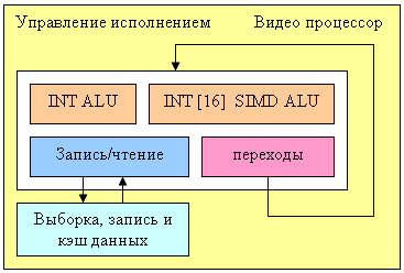
This is the separate programmed NV40 unit that is charged with processing video flows:
The processor contains four functional units (integer ALU, vector integer ALU with 16 components, data loading and unloading unit, and a unit controlling jumps and conditions) and thus can execute up to four different operations per clock. The data format is integers of 16-bit or 32-bit precision (it is not known more exactly which, but 8 bits wouldn't be enough for some algorithms). For more convenience, the processor includes special possibilities of data flow selection, commutation, and writing. Such classical tasks as video decoding and coding (IDCT, deinterlacing, colour model transformations, etc.) can be executed without the CPU. But still, a certain amount of CPU control is required: it is the CPU that has to prepare data and transform parameters, especially in complex algorithms of compression that include unpacking as one of the interim steps.
Such processor can relieve the CPU of many operations, especially in the case of hi-res videos, such as increasingly popular HDTV formats. Unfortunately, it is not known if the processor's capabilities are used for 2D graphic acceleration, especially for some really complex GDI+ functions. But anyway, NV40 meets the requirements for hardware 2D acceleration: all necessary computive intensive GDI and GDI+ functions are executed hardwarily.
OpenGL extensions and D3D features
Here's the list of extensions supported by OpenGL (Drivers 60.72):
- GL_ARB_depth_texture
- GL_ARB_fragment_program
- GL_ARB_fragment_program_shadow
- GL_ARB_fragment_shader
- GL_ARB_imaging
- GL_ARB_multisample
- GL_ARB_multitexture
- GL_ARB_occlusion_query
- GL_ARB_point_parameters
- GL_ARB_point_sprite
- GL_ARB_shadowGL_ARB_shader_objects
- GL_ARB_shading_language_100
- GL_ARB_texture_border_clamp
- GL_ARB_texture_compression
- GL_ARB_texture_cube_map
- GL_ARB_texture_env_add
- GL_ARB_texture_env_combine
- GL_ARB_texture_env_dot3
- GL_ARB_texture_mirrored_repeat
- GL_ARB_texture_non_power_of_two
- GL_ARB_transpose_matrix
- GL_ARB_vertex_buffer_object
- GL_ARB_vertex_program
- GL_ARB_vertex_shader
- GL_ARB_window_pos
- GL_ATI_draw_buffers
- GL_ATI_pixel_format_float
- GL_ATI_texture_float
- GL_ATI_texture_mirror_once
- GL_S3_s3tc
- GL_EXT_texture_env_add
- GL_EXT_abgr
- GL_EXT_bgra
- GL_EXT_blend_color
- GL_EXT_blend_equation_separate
- GL_EXT_blend_func_separate
- GL_EXT_blend_minmax
- GL_EXT_blend_subtract
- GL_EXT_compiled_vertex_array
- GL_EXT_Cg_shader
- GL_EXT_depth_bounds_test
- GL_EXT_draw_range_elements
- GL_EXT_fog_coord
- GL_EXT_multi_draw_arrays
- GL_EXT_packed_pixels
- GL_EXT_pixel_buffer_object
- GL_EXT_point_parameters
- GL_EXT_rescale_normal
- GL_EXT_secondary_color
- GL_EXT_separate_specular_color
- GL_EXT_shadow_funcs
- GL_EXT_stencil_two_side
- GL_EXT_stencil_wrap
- GL_EXT_texture3D
- GL_EXT_texture_compression_s3tc
- GL_EXT_texture_cube_map
- GL_EXT_texture_edge_clamp
- GL_EXT_texture_env_combine
- GL_EXT_texture_env_dot3
- GL_EXT_texture_filter_anisotropic
- GL_EXT_texture_lod
- GL_EXT_texture_lod_bias
- GL_EXT_texture_mirror_clamp
- GL_EXT_texture_object
- GL_EXT_vertex_array
- GL_HP_occlusion_test
- GL_IBM_rasterpos_clip
- GL_IBM_texture_mirrored_repeat
- GL_KTX_buffer_region
- GL_NV_blend_square
- GL_NV_centroid_sample
- GL_NV_copy_depth_to_color
- GL_NV_depth_clamp
- GL_NV_fence
- GL_NV_float_buffer
- GL_NV_fog_distance
- GL_NV_fragment_program
- GL_NV_fragment_program_option
- GL_NV_fragment_program2
- GL_NV_half_float
- GL_NV_light_max_exponent
- GL_NV_multisample_filter_hint
- GL_NV_occlusion_query
- GL_NV_packed_depth_stencil
- GL_NV_pixel_data_range
- GL_NV_point_sprite
- GL_NV_primitive_restart
- GL_NV_register_combiners
- GL_NV_register_combiners2
- GL_NV_texgen_reflection
- GL_NV_texture_compression_vtc
- GL_NV_texture_env_combine4
- GL_NV_texture_expand_normal
- GL_NV_texture_rectangle
- GL_NV_texture_shader
- GL_NV_texture_shader2
- GL_NV_texture_shader3
- GL_NV_vertex_array_range
- GL_NV_vertex_array_range2
- GL_NV_vertex_program
- GL_NV_vertex_program1_1
- GL_NV_vertex_program2
- GL_NV_vertex_program2_option
- GL_NV_vertex_program3
- GL_NVX_conditional_render
- GL_SGIS_generate_mipmap
- GL_SGIS_texture_lod
- GL_SGIX_depth_texture
- GL_SGIX_shadow
- GL_SUN_slice_accum
- GL_WIN_swap_hint
- WGL_EXT_swap_control
D3D parameters can be ssen here:
D3D RightMark: NV40, NV38, R360
DX CapsViewer: NV40, NV38, R360
Attention! Be advised that the current DirectX version with the current NVIDIA (60.72) drivers does not yet support the capabilities of pixel and vertex shaders 3.0. Perhaps the release of DirectX 9.0c will solve the problem, or perhaps, the current DirectX will be suitable, but only after programs are recompiled using new SDK version libraries. This recompilation will be available soon.
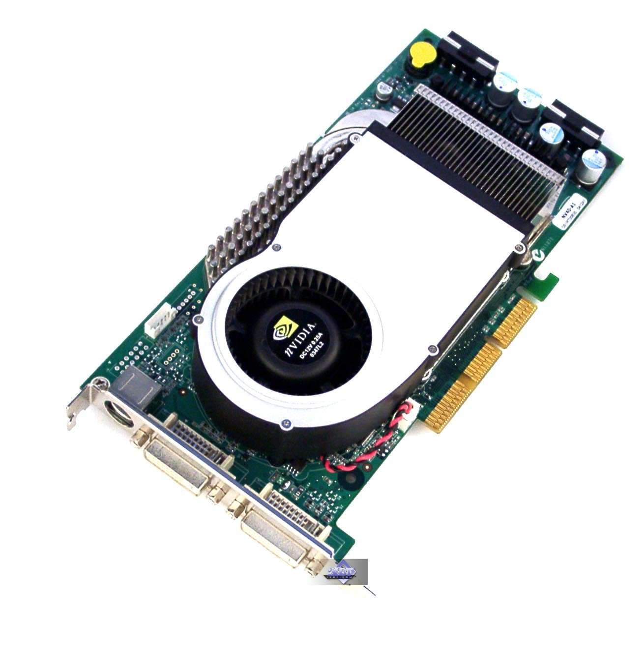
Board
|
NVIDIA GeForce 6800 Ultra 256MB
|

|
NVIDIA GeForce 6800 Ultra 256MB |
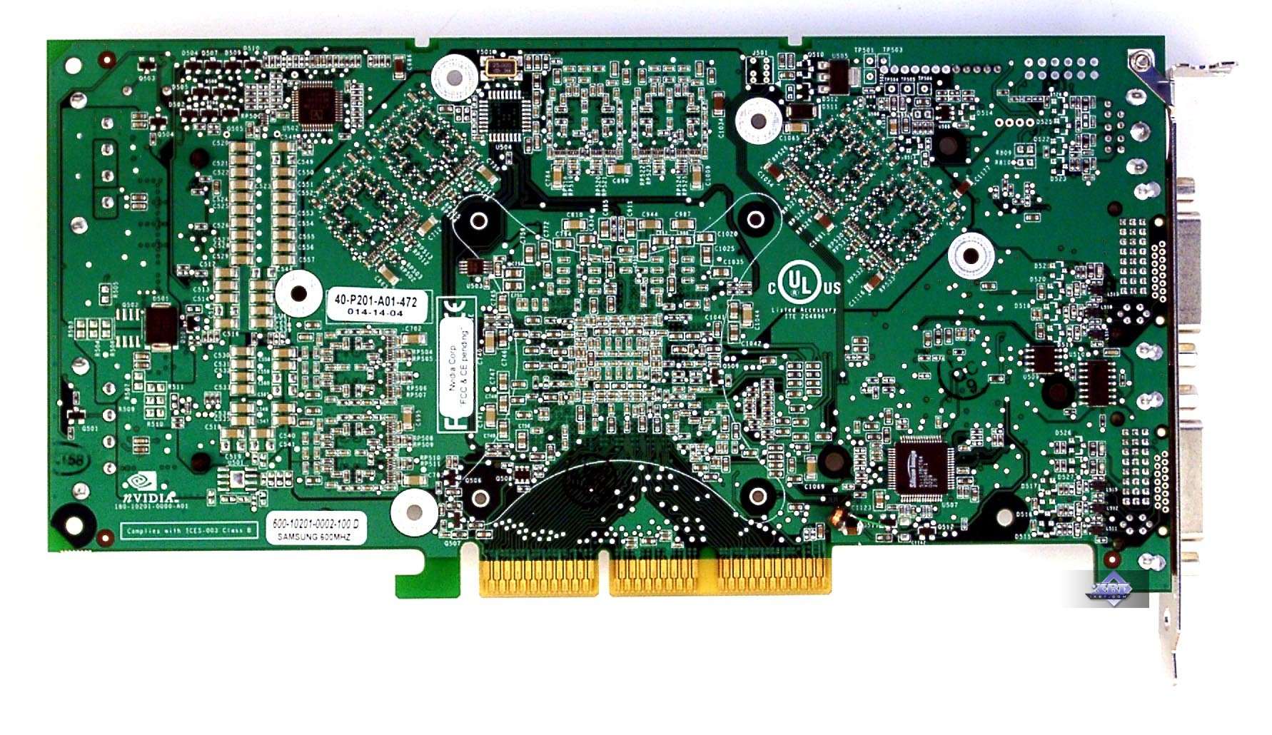
The card has an AGP x8/x4 interface, a 256-MB GDDR3 memory allocated in 8 chips on the front side of the PCB.
The chips are of Samsung make (marking K4J55323QF). Access time is 1.6ns, which corresponds to a 600(1200)-MHz frequency, while the memory works at 550 (1100) MHz. GPU frequency is 400 MHz. Memory interface is 256 bits. |

|
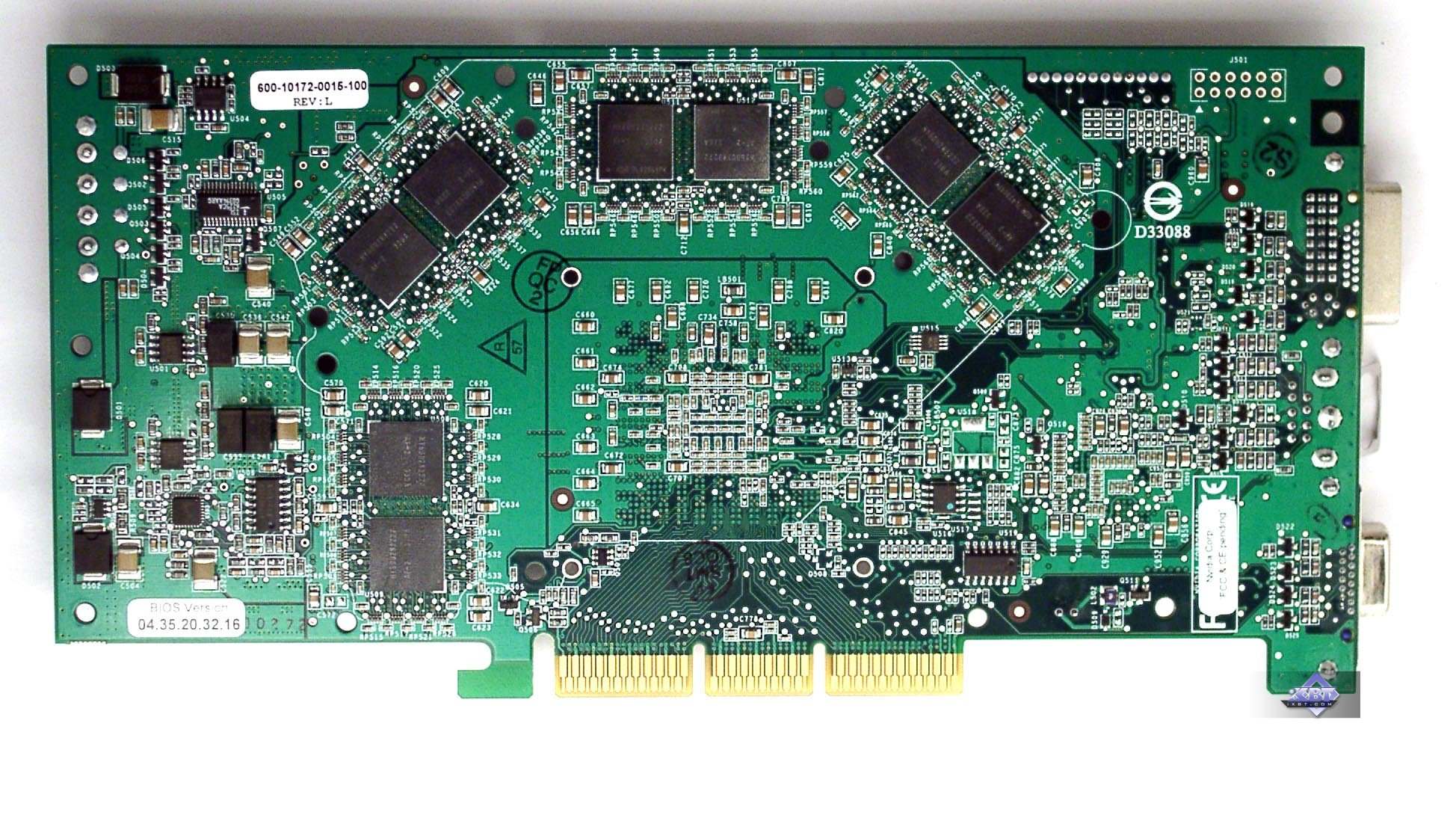
| Comparison with GeForce FX 5950 Ultra, front
view |
| GeForce 6800 Ultra |
Reference card GeForce FX 5950 Ultra |

|

|

|
| Comparison with GeForce FX 5950 Ultra, back
view |
| GeForce 6800 Ultra |
Reference card GeForce FX 5950 Ultra |

|

|

|
|
Evidently, the card design has been changed greatly. Using GDDR3 memory enabled to allocate all the 256 MB on the front side of the board. Thus, it may be possible in the future to supply the card with 512 MB of video memory (providing the PCB will be changed, as the front side of the board has no additional "seats" for another 256 MB, despite the opposite first-sight impression. However, a larger picture shows that the situation as is not the same as was with GeForce FX 5900 non-Ultra. The latter had no memory chips on the back side, although it had the seats for it).
Then we'd like to draw your attention at the power system that has suffered fundamental changes too. Besides a more compact form and a second power connector, the card has made a small revolution: NVIDIA now advises that GeForce 6800 Ultra be used with PSUs no less powerful than 480 W! And that could seriously hamper the card's maket distribution.
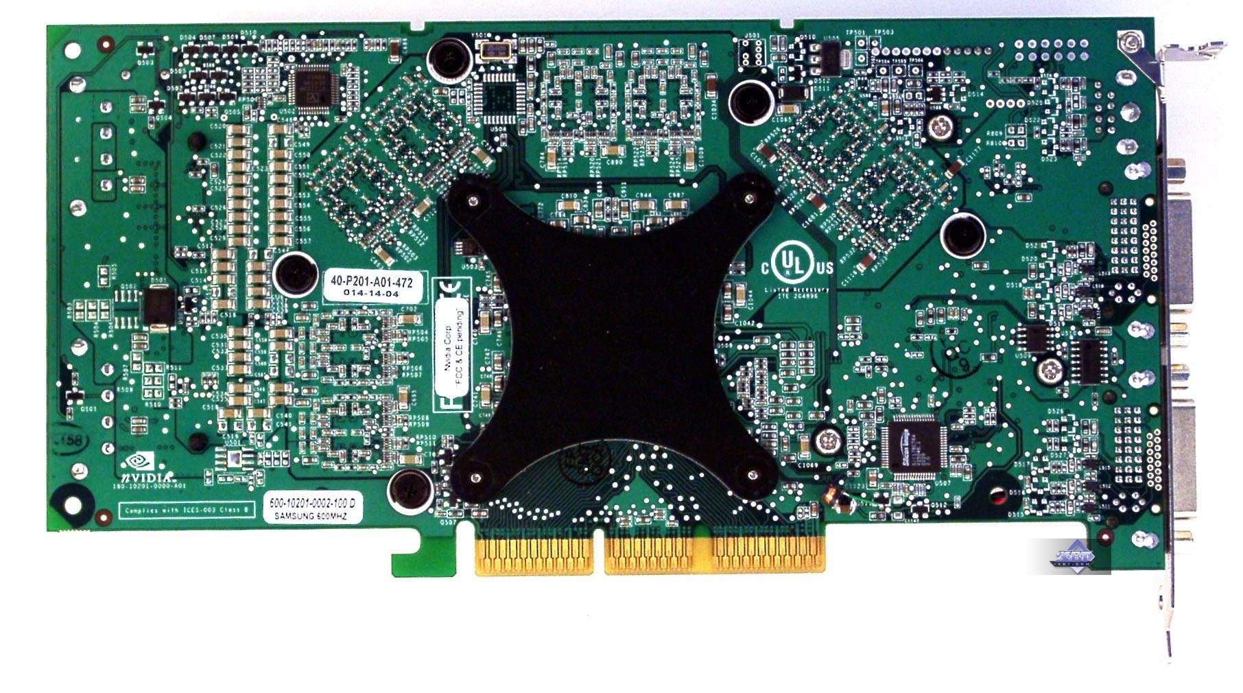
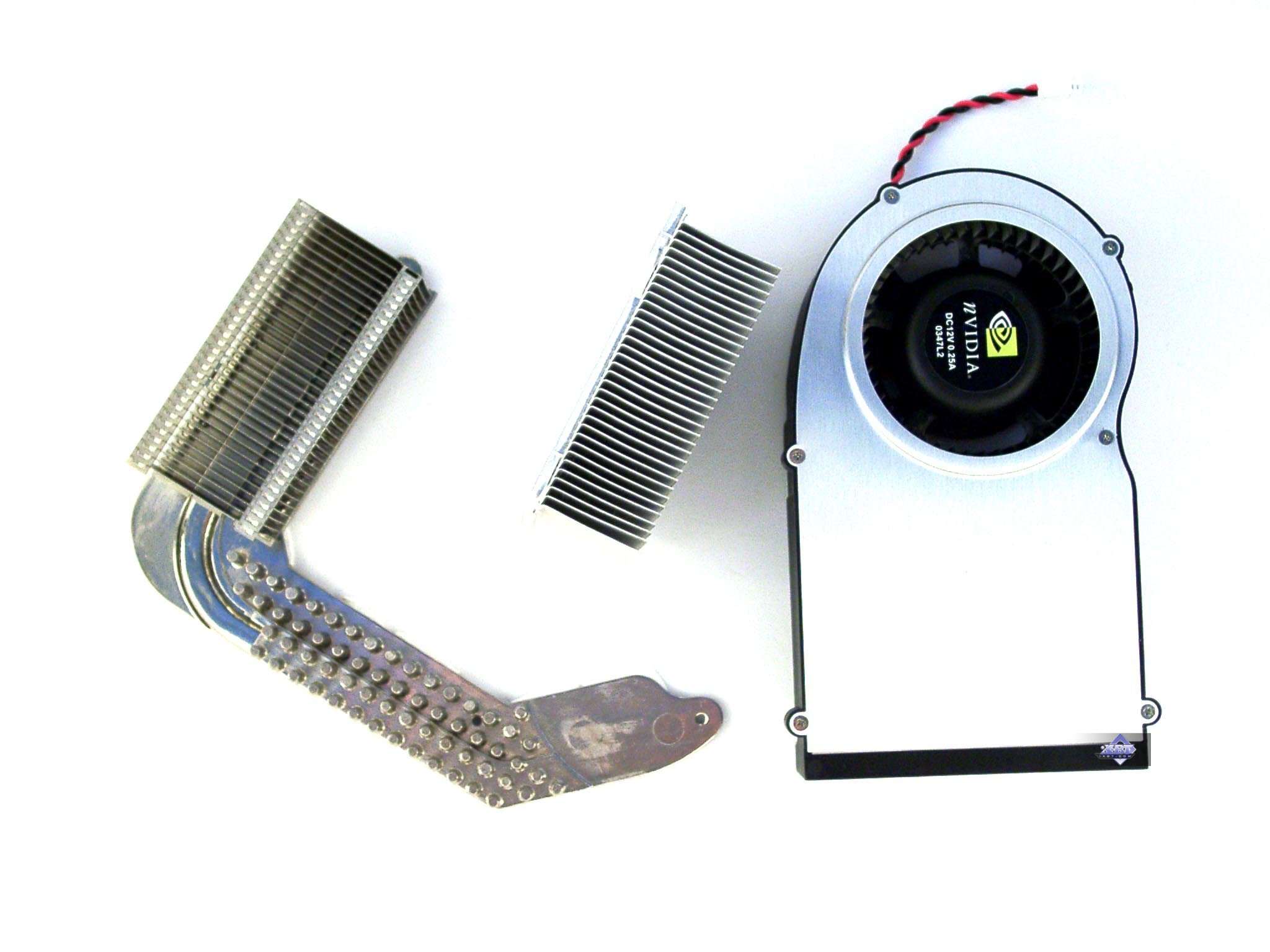
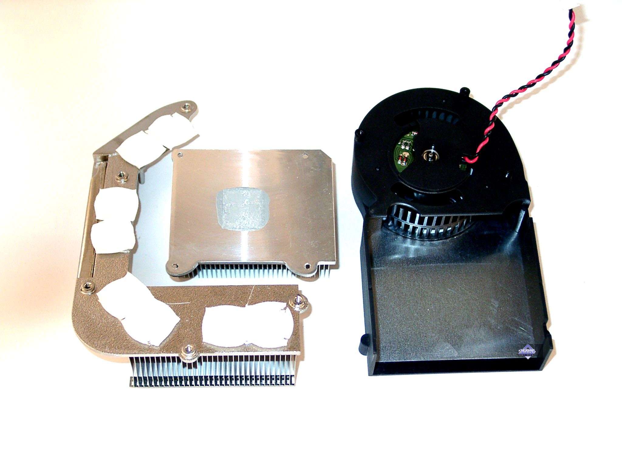
Now let's take a look at the cooling system:
NVIDIA GeForce 6800 Ultra |
| In fact, it is a gradual evolution of the 5950 Ultra cooling system. The only difference is that the air is taken from the inside, not the outside of the case. Besides, the memory cooling system now has a heat pipe that ensures a quicker heat diversion from to chips to the massive needle heatsink. In general the card cooling can be called effective.
Also noteworthy, chances are vendors will use the coolers that do not occupy the AGP-neighbouring slot. |

|

|
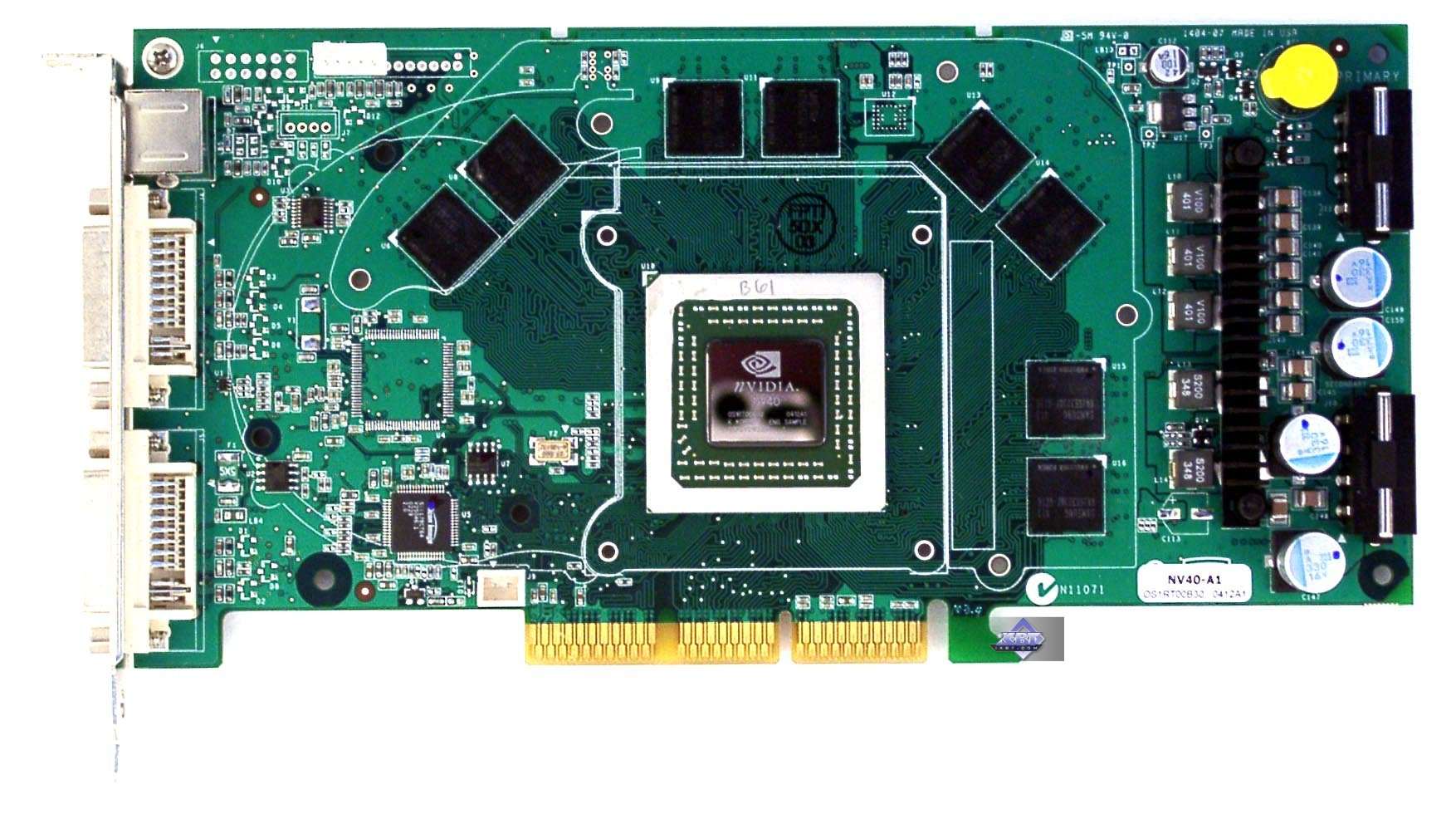
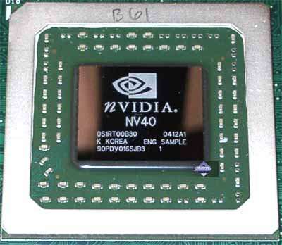
Since we took off the cooler, let's have a closer look at the GPU:
What catches the eye first of all is a huge die: 16 pipelines and 222 million transistors. Another innovation is a frame similar to that used by ATI for protecting their GPU cores from damaging. A die as large as that in NV40 certainly needs such protection.
At this point we finish our description of the card and proceed to the tests.
D3D RightMark synthetic tests
The version of D3D RightMark Beta 4 (1050) synthetic benchmark we used, as well as its description is available at http://3d.rightmark.org
Testbed configurations:
- Pentium 4 3200 MHz based computer;
- Intel Pentium 4 3200 MHz CPU;
- ASUS P4C800 Delux (i875P) mainboard;
- 1024 MB DDR SDRAM;
- Seagate Barracuda IV 40GB HDD;
- Windows XP SP1; DirectX 9.0b;
- ViewSonic P810 (21") è Mitsubishi Diamond Pro 2070SB (21") monitors;
- NVIDIA drivers version 60.72;
- ATI drivers version 6.436 (CATALYST 4.4).
First, let's see whether the announced features (16 pixels per clock, 16 TMUs, etc.) are really such.
Pixel Filling test
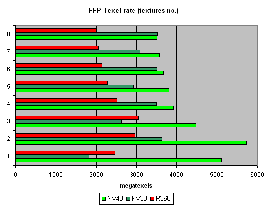
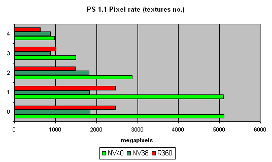
Texelrate, FFP mode, for various numbers of textures overlaid on one pixel:
A theoretical NV40 maximum for this test is 6.4 gigatexels per second. In reality, we nearly reached 6 gigatexels, which clearly indicates that there are 16 texture modules. One texture has a result just a bit lower than two textures have - obviously, the frame buffer bandwidth is not enough, and then we see a steady relation: the more textures, the lower the filling speed. There are no jumps between even and odd numbers (as NV38 has), which is typical of two-TMUs-per-pixel configurations. On the contrary, the picture is similar to that in R360. Thus, we can conclude that the 16x1 scheme has really withstood the reality test. Interestingly, R360 reaches the maximum on three textures, while NV40 only on two, which indicates the latter's more effective work with the frame buffer during filling. And it is no less interesting that as the number of textures grows, NV38 gets closer to NV40 - if there is an even number of textures, the NV38 selection efficiency nearly reaches the theoretical limit. But we remember that real tasks make it much more complicated: R360, not very good at texture selection, often beat NV38 by its number of pipelines and computational capability. We'll examine this aspect of NV40 a bit later.
And right now for the fillrate (pixelrate), FFP mode, for various numbers of textures overlaid on one pixel:
Well, NV40 is the new tzar here. Its peak speed of work with the frame buffer (0 textures -colour filling and one texture) is twice as high as in R360 and 2.5 times higher than in NV38. However, this chip rights itself with an even number of textures (2 and more). And although the theoretical limit of 6.4 gigapixels per second is not reached, it is definitely possible to write 16 pixels per clock. Thus, as many as 4 quads (2x2) (i.e. 16 pixels) are processed per clock. Interestingly, as the number of textures grows, the filling speed falls faster than in the previous generation: this is due to a low core frequency and a double number of texture units compared to a fourfold increase in the number of pixels.
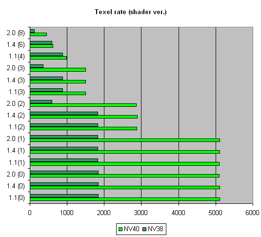
Let us look at the relation between the filling speed and the shader version:
the picture is same as with FFP.
Ironically, NVIDIA is now an undisputable leader on shaders 1.4, ATI's brain-child. Well, life is life.
Due to its architectural peculiarities, NV38 slowed down on shaders 2.0 in this test (additional clocks were needed for some instructions realised as macros in NV38), which made it more effective with shaders 1.4 (although it is exactly the opposite with R360 where 2.0 has a higher performance than 1.4). But now the justice is restored, miscalculations are corrected, and NV40 is equally good on all shader versions. Though we must say old R360 looks not at all so bad against NV40.
Here is a summary graph for a number of textures, that compares NV38 and NV40:
Thus, the following preferrences can be noticed:
| Version |
1.1 |
1.4 |
2.0 |
| NV40 |
Optimal |
Optimal |
Optimal |
| NV38 |
Optimal |
Optimal |
Not optimal |
| R360 |
Optimal |
Not optimal |
Optimal |
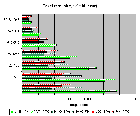
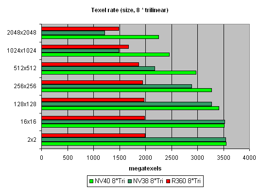
And now let's see how well texture modules cope with caching and bilinear filtering of real different-size textures:
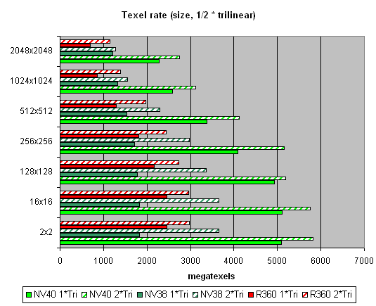
The data are given for textures of different sizes, one and two textures per pixel. Concerning sizes up to 512x512, 16 NV40 texture modules have a visible advantage there, and their results are close to the theoretical limit. But then, as the texture sizes grow, the memory bandwidth becomes the restrictor. Caching efficiency is really high: we reach more than 4 gigatexels on the most common size of 128x128. Now let's see how things will change at trilinear filtering:
Gee! NV40's advantage is even more solid here. But that makes sense: the more texture units, the higher the results of trilinear filtering. And besides, mip levels enable a more effective texture data caching. NV40 has a double advantage here, which means it's got no rivals in this aspect.
And finally, here's a limiting case of 8 textures subjected to trilinear filtering:
It shows once again that realisation of texture selection is NVIDIA's strong point.
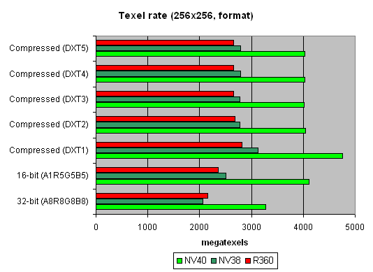
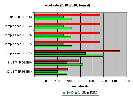
Andnow let's take a look at the relation between performance of texture modules and texture formats:
A larger size:
That's pretty interesting, isn't it? Why does R360 defeat even NV40 when compressed textures have larger sizes? The answer is simple as that: textures stored in an NVIDIA texture cache are already unpacked and made into the 32-bit format, while an ATI texture cache contains textures that are still compressed. On one hand, NVIDIA must have a more effective texture selection, as there are fewer standstills during unpacking and consequently, less time is spent. But on the other hand, a large size of the textures can bring about ATI's leadership, as NV40 will reach the maximal memory bandwidth and even its 16 TMUs won't help it. And that is, actually, what we see in the second graph. In real applications, however, the balance can tilt to either side, depending on the shaders, the number of textures and their size, and on many other parameters.
Si, ibn general, two facts can be stated:
- NV40 is a champion in texture filling and selection: 16 pixels per clock, 16 TMUs, and a legendary effectiveness of NVIDIA's TMUs and frame buffer is still the same.
- NVIDIA's previous instability on shaders 2.0 has been eliminated.
Geometry Processing Speed test
The simplest shader - the maximal triangle bandwidth:
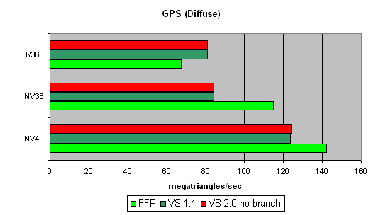
It's difficult to say why NV40's results do not exceed those of the previous generation. To all appearance, the chip's vertex processors just can't make a full flip on such a primitive task. Later we will check our assumption on more complex tasks. And now we can state that NV40's speed dependence on the shader version coincides with that in NV38, and as was supposed before, the vertex processors of these chips may have a lot in common.
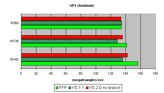
A more complex shader - one simple point light source:
Here, NV40's advantage becomes more visible. A too short shader was just limited by the speed of the buffers and the vertex selection mechanism, while the NV40's vertex processor had the opportunity to be engaged in calculations, and the result was quick to improve. Interestingly, FFP is still the best variant for NVIDIA and the worst one for ATI, due to additional units designed for a quicker lighting calculation within standard FFP requirements.
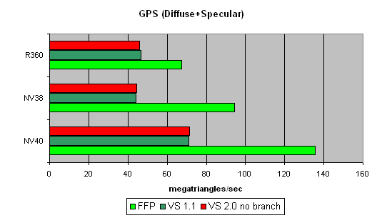
Let's make the task still more complicated:
FFP leads here even with ATI: it algorithm is simpler than that used in the vertex shader. And NV40 is a clear-cut champion here.
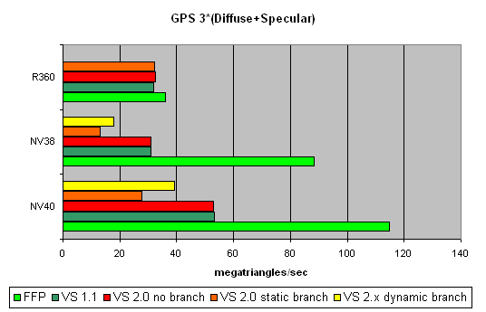
And now the most complex task: three light sources in variants without jumps, with a static and a dynamic exeution control:
Static jumps badly affect NVIDIA. And as the decrease is similar in both NV38 and NV40, we can conclude that their vertex processors are also similar (in this respect). The paradox is that dynamic jumps are better than static ones for NVIDIA chips. In the case of ATI, everything is quite smooth.
Thus, to conclude:
- FFP are much faster (often two times faster) on NVIDIA chips.
- NV38 and NV40 have a similar dependence on the shader version - evidently, the architectures of their vertex processors are very much alike.
- Static jumps do not have an optimal execution on NVIDIA accelerators.
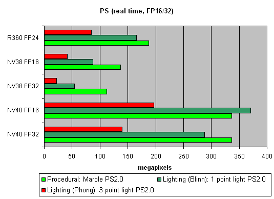
Pixel Shaders test
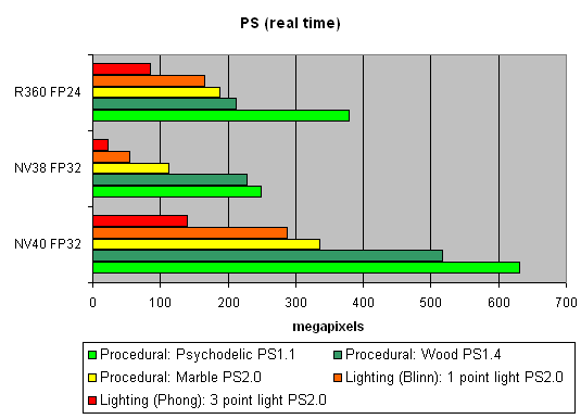
The first group of shaders are versions simple for real-time execution: 1.1, 1.4, and 2.0:
Well, that's finally it: NV40 has defeated NV38. The new layout of the pixel processor, new ALUs and texture module cope excellently with different shader versions.
Let's find out the increase of using 16-bit precision floating-point numbers:
16-bit precision brings NV40 an advantage, bigger in some shaders, smaller in others, and sometimes even more visible than for NV38. Of course, it may be due to the compiler's influence: the more optimised it will get, the fewer temporary variables and pixel processor rounds will be used. As a result, the difference may diminish and FP32 results will get closer to FP16.
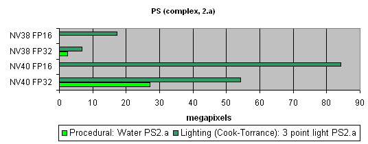
Now let's take a look at really complex "cinema" shaders:
NV40 shows a fantastic performance, several times higher than the results of the previous generation. Dozens of dependent texture selections, a multitude of temporary variables, a complex code - that's why the difference between 16 and 32 bits is so great.
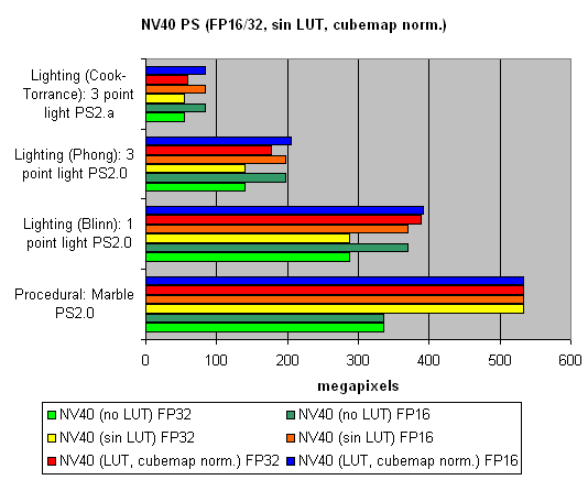
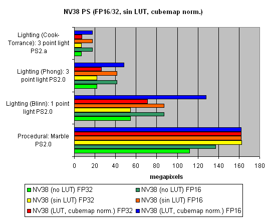
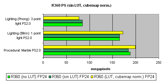
And finally, we will examine how speed is dependent on arithmetic or diagram methods of sin, pow calculation and vector normalisation. We will do it separately for each chip:
The general conclusions are as follows:
- 16 bits are better than 32 bits.
- Tables are better than arithmetic calculations for NVIDIA(an effective texture selection).
- Calculations are better than tables for ATI (a less effective texture selection).
Total results for pixel shaders:
- Performance is beyond comparison, a sad experience of the previous generation is a thing of the past.
- Dynamic control of calculations didn't worsen the performance of standard shaders.
- Weak points (in respect of temporary variables) are corrected, but a certain growth can still be expected of the compiler in future driver versions, as the compiler is not so effective as in NV38.
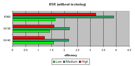
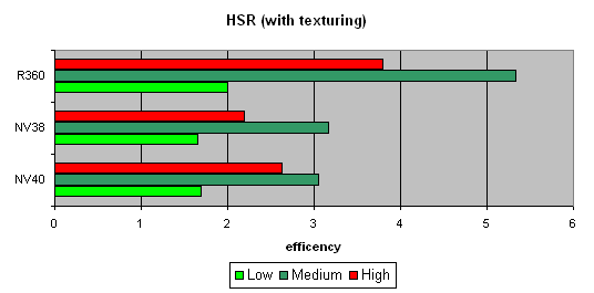
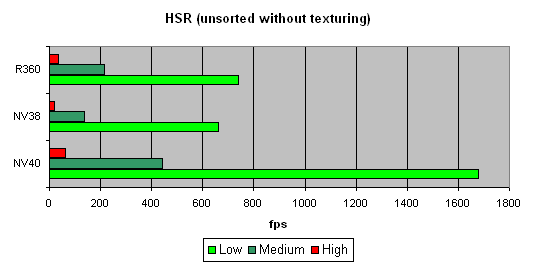
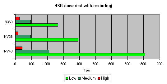
HSR test
We will begin with the peak efficiency (with and without textures) depending on the geometrical complexity:
It is clear that ATI is better in moderate and complex scenes, due to two levels of reduced Z buffers (except the base buffer). NVIDIA traditionally has an additional level, which results in a lower HSR efficiency in the case of an optimal scene balance (moderate complexity). Besides, more effective filling and texturing also reduce peak HSR efficiency (or, to be more precise, the penalty for not removed areas diminishes).
The dependence character shows that ther have been no changes in the algorithm since NV38. But absolute figures have increased substantially:
NV40 is evidently beyond comparison being at least twice as good as others.
Conclusion:
- The HSR algorithm has underwent no major changes.
- But its general performance has increased, which is normal if we consider the increased number of removed quads per clock.
Point Sprites test.
We think, our readers are smart enough to make conclusions themselves. Sprites ceased to be a popular innovation long time ago and often lose to triangles in rendering speed.
Quality of trilinear filtering and anisotropy
|
Trilinear filtering (Angle 0) |
GeForce FX 5950 Ultra |
GeForce 6800 Ultra |
RADEON 9800XT |
High Quality |
- |

|

|
Quality |

|

|

|
Performance |

|

|

|
High Performance |

|

|

|
Trilinear filtering (Angle 30) |
GeForce FX 5950 Ultra |
GeForce 6800 Ultra |
RADEON 9800XT |
High Quality |
- |

|

|
Quality |

|

|

|
Performance |

|

|

|
High Performance |

|

|

|
Trilinear filtering (Angle 45) |
GeForce FX 5950 Ultra |
GeForce 6800 Ultra |
RADEON 9800XT |
High Quality |
- |

|

|
Quality |

|

|

|
Performance |

|

|

|
High Performance |

|

|

|
Trilinear filtering (Angle 60) |
GeForce FX 5950 Ultra |
GeForce 6800 Ultra |
RADEON 9800XT |
High Quality |
- |

|

|
Quality |

|

|

|
Performance |

|

|

|
High Performance |

|

|

|
Trilinear filtering (Angle 90) |
GeForce FX 5950 Ultra |
GeForce 6800 Ultra |
RADEON 9800XT |
High Quality |
- |

|

|
Quality |

|

|

|
Performance |

|

|

|
High Performance |

|

|

|
Anisotropic filtering (Angle 0) |
GeForce FX 5950 Ultra |
GeForce 6800 Ultra |
RADEON 9800XT |
Anisotropic 0x |

|

|

|
Anisotropic 8x |

|

|

|
Anisotropic 16x |
- |

|

|
Anisotropic filtering (Angle 30) |
GeForce FX 5950 Ultra |
GeForce 6800 Ultra |
RADEON 9800XT |
Anisotropic 0x |

|

|

|
Anisotropic 8x |

|

|

|
Anisotropic 16x |
- |

|

|
Anisotropic filtering (Angle 45) |
GeForce FX 5950 Ultra |
GeForce 6800 Ultra |
RADEON 9800XT |
Anisotropic 0x |

|

|

|
Anisotropic 8x |

|

|

|
Anisotropic 16x |
- |

|

|
Anisotropic filtering (Angle 60) |
GeForce FX 5950 Ultra |
GeForce 6800 Ultra |
RADEON 9800XT |
Anisotropic 0x |

|

|

|
Anisotropic 8x |

|

|

|
Anisotropic 16x |
- |

|

|
Anisotropic filtering (Angle 90) |
GeForce FX 5950 Ultra |
GeForce 6800 Ultra |
RADEON 9800XT |
Anisotropic 0x |

|

|

|
Anisotropic 8x |

|

|

|
Anisotropic 16x |
- |

|

|
|
The mip-level selection algorithm is different from that in NV38. Piecewise-linear approximation is now executed with more segments, which is a positive change. But NV38 used a more precise (probably, quadratic) approximation for planes at 0° and 90° (floor and walls) than for other angles. And that makes NV38 a bit superior than NV40 concerning this important and widespread case. In other cases, however, NV40 ensures a much better approximation of an ideal curve. Besides, the zones for real execution of trilinear filtering became more extended. NV38 had more aggressive settings, which was probably caused by its lag from R3XX in various tests. However, after the release of R420, new drivers may appear with more aggressive NV40 settings too - settings that will be speed-oriented, not quality-oriented. And concerning R360, it has fewer lines that approximate the curve isoline of distance to the viewer, but more extended zones for trilinear filtering. Is it good or bad? Well, screenshots of real game applications can show, but it's an obvious fact that there is a difference.
The anisotropic algorithm has changed. It's difficult to tell the extent of the changes, but the algorithm has definitely become closer to ATI. Some critical angles are marked by a higher blurring, some give the opposite impression that NV40 ensures a sharper picture than NV38, and that makes its behaviour similar to R360, though there is a difference between them in specific moments. The fact that anisotropic filterings are different in NV38 and NV40 may be largely due to the changes in the algorithm of mip-level selection.
The second part of the article will feature the influence of this fact on graphic quality of specific applications.
Conclusions
- Mistakes have been corrected.
- A solid foundation for the future has been made.
- Performance is beyond comparison (for the moment).
- NV40 looks better to us than NV30 when it was announced.
But to make ultimate conclusions, we are waiting for the following things:
- The release of ATI R420
- The results of the game tests
- A possibility to test in comparison performance and AA and anisotropic quality of NV40 and R420
- A possibility to use shaders 3.0 and to test their perfomance.
|
| |