|
||
|
||
| ||
|
||
|
||
| ||
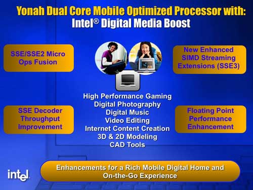
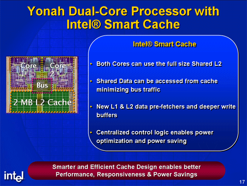
The last but not the leastWe have finally seen the launch of the last representative of the long-playing Pentium Pro series — Pentium II — Pentium III — Pentium M, which history goes back more than ten years (since 1995 to 2006). It's launched under a strange and lightweight name - Intel Core Duo. But it does not change its essence: it's still a Pentium M — but highly modified and implemented as a dual core processor with a shared L2 Cache. 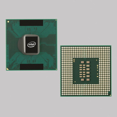 In order not to stand out in the row of common P6 CPU names and to highlight noticeable microarchitectural differences of the new processor from its immediate predecessor Pentium M (Dothan), we'll call it Pentium M2 in this article. We'll also use abbreviations for all processors in this series: PPro, P-II, P-III, P-M, P-M2. But at first let's agree upon the terminology due to ambiguous "dual-core" and "dual-processor" notions. Following Intel's example, the following interpretation is used in popular literature: everything in a single package (and inserted into a single socket) is called a processor, each of two devices in this package (not necessarily on the same die), not connected with each other on the microarchitectural level and executing separate instruction flows, is called a core. On the other hand, each of these cores is a sterling processor in the strictest sense of this word. For example, IBM uses only strict terminology: two processors on one POWER4 chip. That's why in order to avoid ambiguity and not digress from the emergent terminology, we shall use the term "processor core" or "CPU" meaning each independent processor and "processor chip" or "socket" meaning a dual-core processor proper. In this connection, a system with two processor sockets should be called dual socket rather than dual processor system (irregardless of the number of cores in each processor chip). This terminology issue wasn't elaborated in the previous article about dual core processors of the new architecture, which roused some censure. 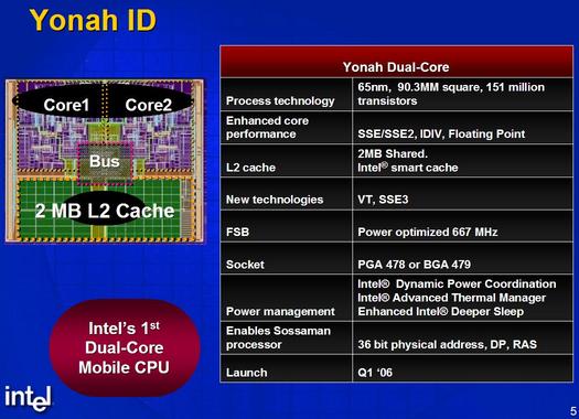 The key properties of the dual core Yonah are shown on the image above. The new processor does not contain anything special on the face of it. Expectable die size for the 65-nanometer process technology, expectable shared 2 MB L2 Cache, expectably improved power consumption technologies. The clock frequency is also quite expectable — 2.16 GHz now and 2.33 in the second quarter. But if we dig deeper, we'll see that Yonah has surprisingly many important microarchitectural differences from its predecessor, P-M processor on Dothan core. Information about them appeared back in Spring and Autumn IDF-2005, but it was overlooked on the background of news about the new Merom/Conroe CPU architecture. Most interestingly, there were no signs of such microarchitectural changes for mobile use. I guess Intel has chosen a path of careful evolutionary development of the existing P6+ (P-M) architecture, in order to streamline various innovations before introducing them into next-gen Merom/Conroe processors. These innovations may quite possibly fail to make a significant contribution into performance growth, as they don't touch many weak spots of the P-III/P-M architecture. But they have to do with those processor blocks, which seemed critical to the future high-performance architecture and about which we made various assumptions. In this article the new processor will be reviewed mainly from the microarchitectural point of view — that is in operational terms of internal processor units and execution efficiency of user applications. Such characteristics and innovations as power management and virtualization technology (VT) will be just briefly mentioned. What's been changed?
|
|
Processor
|
Codename
|
Process, µm
|
L1 I/D Caches
|
L2 Cache
|
|
P Pro
|
P6
|
0.5
|
8/8
|
256
|
|
P-II
|
Deschutes
|
0.25
|
16/16
|
512
|
|
P-III
|
Tualatin
|
0.13
|
16/16
|
512
|
|
P-M
|
Dothan
|
0.09
|
32/32
|
2048
|
|
P-M2
|
Yonah
|
0.065
|
32/32
|
2048
|
|
Processor
|
Form-factor
|
Clock, GHz
|
Architectural enhancements
|
Microarchitectural improvements
|
|
P Pro
|
Assembly
|
0.20
|
+conditional operations
|
New microarchitecture
|
|
P-II
|
External L2
|
0.45
|
+MMX
|
External L2, improved 16-bit
|
|
P-III
|
|
1.40
|
+SSE
|
Fast L2,
prefetch |
|
P-M
|
|
2.26
|
+SSE2
|
µop fusion, improved branch prediction
|
|
P-M2
|
2 cores
|
2.33
|
+SSE3
|
SSE µop fusion, shared L2 cache
|
We have come to a conclusion that Yonah can be reviewed as a transition model that is created to streamline various innovations before introducing them into next-gen Merom/Conroe processors. And now let's see what features of the future processor have been already implemented and what features are yet to be added. Of course, we are speaking of only those subsystems that could have been improved in processors of the old P6 architecture and that wouldn't have required a radical overhaul of the processor structure. Such fundamental issues as the increased number of decoded and processed instructions from three to four as well as support for 64-bit EM64T (x86-64) mode require considerable overhauling of many subsystems and units. So they couldn't appear in the process of evolution.
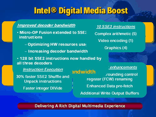
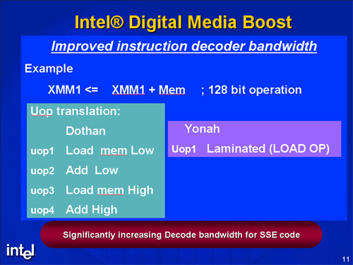
In the previous article about processors of the new architecture we reviewed various subsystems of a processor from the point of view of the necessity to improve them. The main emphasis was made on the necessity to overhaul the decoder in order to support all micro-op fusion modes and to provide a necessary speed of generating SSE micro-ops. Judging from the Yonah review, we can draw a conclusion that the problem was successfully solved. Moreover, it's solved in the most efficient way, including conversion of the most complex SSE instruction — packed (128-bit) Load-OP — into a single macro-op.
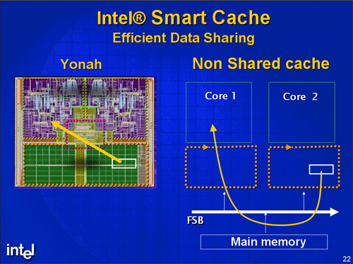
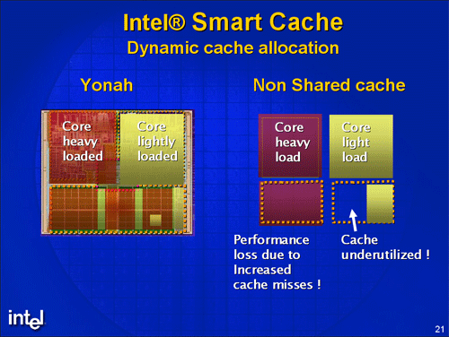
Besides, there appeared another fundamental element of the new architecture — shared (between two processor cores) L2 Cache. Plus improved power management and VT support.
What else must be changed in processors of the new architecture, in order to provide a necessary performance and competition level? It's evidently a floating point unit. At minimum — to implement a full-frequency 64-bit multiplication. Proceeding from the fact that such an improvement was added to Pentium 4 processor, operating at a much higher clock frequency, no doubt that it can be easily done in the new architecture. But in this case, floating point performance will be inferior to performance of the old family (Pentium 4).
Thus we can assume (it's confirmed by some sources) that Merom/Conroe processors will have 128-bit full-frequency floating point SSE arithmetic for all operand types. Within this assumption, multiplication and addition units will become wider and retain their full frequency. That is each of them will be able to output one 128-bit result per cycle — to be more exact, two 64-bit (SSE2) or four 32-bit (SSE) results in packed operations. But still one operation of each type (multiplication and addition) per cycle will be executed in scalar mode. Thus, in scalar mode the new processor will just catch up (in formal FPU speed) with AMD K8 — but in packed mode it will outperform it twofold, reaching the peak performance of quad clock frequency on 64-bit arithmetic.
The assumed doubled maximum performance must be supported by the instruction decoder — as we have already seen above, the decoder can output a necessary number of 128-bit µops (to reach maximum FPU speed, 2 such µops are required in each cycle with the total width of CPU lanes equal to four). Besides, the doubled performance will require an increased speed of reading data from L1 Cache providing (at least) one 16-byte reading per cycle.
We have information that the new processors will have an additional floating point instruction set, which may be called SSE4. Like the previous SSE3, the new extension will probably not be an independent instruction set (like SSE or SSE2), but an addition, which will extend some bottlenecks and provide additional flexibility in using the existing instruction sets. For example, we are interested in the ways of improving operation with 64-bit halves of XMM registers for their separate loading/storing, swapping, and other conversions to allow packed SSE2 instructions to be used for processing array groups not aligned to each other with 16-byte multiplicity. The last limitation is a serious obstacle for efficient usage of packed instructions in calculations.
Finally, processors of the new architecture must have a seriously improved Out-of-Order execution mechanism, up to its complete redesign with due regard for the experience from designing Pentium 4 and competing products. The architecture announcement spoke of enlarged buffers. It may also assume a modified structure of such buffers. For example, a possible switch from a system with a single queue (buffer) for macro-ops to a system with several queues, assigned to corresponding functional units. It would have allowed maximum speed of issuing operations for execution without complicating the structure and making a processor cycle longer.
Taking into account the wider processor lanes, there must be an increased number of functional units of some types (integer arithmetic and logic units in the first place) as well as a modified structure of execution ports.
And in conclusion, we should remind you that the new processors will support EM64T (x86-64) mode — that is to contain a full set of 64-bit integer and address units.
Thus, we can draw a conclusion that the microarchitecture of the future Merom/Conroe/Woodcrest processors will be based on the same fundamental principles as the P6/P6+ architecture — but it will be overhauled with regard to many years' experience of competing products, new electronic technologies and new users' requirements. We can say for sure that processors of the new architecture will be more different from their predecessors (P-M/P-M2) than 64-bit AMD K8 processors from their 32-bit predecessors (K7).
In conclusion we'll publish characteristics of some Yonah models. I repeat that this processor got a new name — "Core Duo" for a dual core modification and "Core Solo" for a single core modification. Besides, the designation system for CPU models was also changed. Now it consists of a letter, pointing out the maximum level of power consumption (U — up to 15 Watts, L — up to 25 Watts, T — up to 50 Watts, E — higher than 50 Watts), and a four-digit code, which starts with 1 or 2 (a number of CPU cores). At present top representatives in each series are processors with normal and reduced power consumption - T2600 (2.16 GHz), T1300 (1.66 GHz) and L2400 (1.66 GHz) with a 667 MHz bus as well as models with ultra low power consumption - U2500 (1.06 GHz) and U1400 (1.20 GHz) with 533 MHz bus. Higher-performance models will be released in the second quarter - T2700 (2.33 GHz), T1400 (1.83 GHz) and L2500 (1.83 GHz). There is still no information about E-indexed processors.
A tad later we'll see another modification of this processor, codenamed Sossaman, for servers with reduced power consumption and heat dissipation. This processor supports dual socket configurations (4 CPU cores per system). The new processor supports monitor and mwait instructions for synchronizing processes.
The first Core Duo results demonstrate a good performance level, comparable in single-threaded applications to the P-M (Dothan) level. In multi-threaded applications, it noticeably exceeds it with a similar power consumption level and comes close to the desktop level. For example, SPECint_rate_base2000 and SPECfp_rate_base2000 results, which characterize the execution speed of threads in a multi-processing (multi-core) system, for the top T2600 model (2.16 GHz) are 34.9 and 27.4 correspondingly. For your information, the Pentium XE 955 (3.46 GHz) with 2 x 2 MB cache demonstrates the following results in these tests - 41.1 and 36.6. Two other dual core processors with 2 x 1 MB caches demonstrate lower results: Pentium XE 840 (3.2 GHz) — 33.5 and 31.9, AMD Opteron 280 (2.4 GHz) — 35.9 and 30.8 (in 32-bit mode). Taking into account that Yonah is a transition model on the way to a new architecture, we can draw a conclusion that it's a strong-knit mobile processor, which is no conjurer, but answers our expectations. Thus it was a good decision to entrust this team from a hot country (Israel) with creating such processors. Let's hope that the next Merom/Conroe family, which is designed by the same team, will also come up to our expectations.
Write a comment below. No registration needed!
|
Article navigation: |
| Most Popular Reviews | More RSS |
 |
Comparing old, cheap solutions from AMD with new, budget offerings from Intel.
February 1, 2013 · Processor Roundups |
 |
Inno3D GeForce GTX 670 iChill, Inno3D GeForce GTX 660 Ti Graphics Cards A couple of mid-range adapters with original cooling systems.
January 30, 2013 · Video cards: NVIDIA GPUs |
 |
Creative Sound Blaster X-Fi Surround 5.1 An external X-Fi solution in tests.
September 9, 2008 · Sound Cards |
 |
The first worthwhile Piledriver CPU.
September 11, 2012 · Processors: AMD |
 |
Consumed Power, Energy Consumption: Ivy Bridge vs. Sandy Bridge Trying out the new method.
September 18, 2012 · Processors: Intel |
| Latest Reviews | More RSS |
 |
Retested all graphics cards with the new drivers.
Oct 18, 2013 · 3Digests
|
|
Added new benchmarks: BioShock Infinite and Metro: Last Light.
Sep 06, 2013 · 3Digests
|
|
Added the test results of NVIDIA GeForce GTX 760 and AMD Radeon HD 7730.
Aug 05, 2013 · 3Digests
|
 |
Gainward GeForce GTX 650 Ti BOOST 2GB Golden Sample Graphics Card An excellent hybrid of GeForce GTX 650 Ti and GeForce GTX 660.
Jun 24, 2013 · Video cards: NVIDIA GPUs
|
|
Added the test results of NVIDIA GeForce GTX 770/780.
Jun 03, 2013 · 3Digests
|
| Latest News | More RSS |
Platform · Video · Multimedia · Mobile · Other || About us & Privacy policy · Twitter · Facebook
Copyright © Byrds Research & Publishing, Ltd., 1997–2011. All rights reserved.