 |
||
|
||
| ||
|
||
|
||
| ||
IntroductionA long-awaited event happened the other day — Intel announced at IDF the microarchitecture of IA-32 (x86) processors of the next generation. The new microarchitecture will be the same for all the three classes of processors: mobile, desktop, and server. The key distinguishing features of the new processors are dual cores, EM64T (x86-64) support, active usage of power saving technologies and introduction of Star Technologies (*Ts), streamlined in the latest versions of Pentium 4 and Pentium M processors. The first versions of the new processors — mobile Merom, desktop Conroe, and server Woodcrest — will appear on sale in the second half of 2006. 
Being a votary of the aggressive advertising policy, Intel has tried to present characteristics of its new processors in the most spectacular form. This time the corporation decided to use the Performance/Watt ratio compared to the previous processors as its trump card. Of course, this ratio misleads the readers — but it can still give a general idea of CPU performance. What urged Intel to design a new architecture? The main reasons are obvious: excessive increase of power consumption (and heat dissipation as a result) of Pentium 4 processors, the consequent fashion for economic processors, the halt of the evolutional clock growth that made engineers design dual core processors and introduce them first to social consciousness and then to the open market. Besides, we can probably add to the list such an unobvious factor as the dislike (economically justified!) of software developers to optimize their programs for modern high-frequency microprocessors. As a result, these programs don't get the expectable performance gain from the key architectural innovations in CPUs (it concerns the Pentium 4 processor in the first place). What is the new architecture based on? That's the most interesting question, generating a lot of subjective interpretations. Have a look at the presentation slide below, you will see that the new architecture is allegedly equally based on the previous two architectures: NetBurst (Pentium 4) and Banias (Pentium M). 
However, the list of key elements on the slide, borrowed from these architectures, is too short. It includes only such elements as 64 bit, Star Technologies, power optimizations, and bus; it does not include the main micro architectural features. That's why it seems hard to point out the true "ancestor" of the new architecture. However, it's clear enough that NetBurst (Pentium 4) is not the direct "father" of the new processors — otherwise, its key advantageous characteristics would have been certainly included and highlighted. Hence the question: is the new architecture a heir to the old good Pentium III processor (from the dynasty founded long ago in 1995 by the Pentium Pro grandfather), or is it actually a new architecture, even if based on the key principles of P-III? Is it a step back or a step forward? In order to answer this difficult question, we'll have to have a microscopic examination of those characteristics of the new processors, which were scarcely published in the presentations, and analyze the key peculiarities, advantages and disadvantages of the supposed predecessors — the two related Pentium III and Pentium M processors. Of course, it's not that important whether we come to a conclusion that the Conroe processor is an overhauled version of Pentium M, or we decide that it's a brand new processor, which had been designed from scratch, but had been filled with previous solutions. The main objective is to understand on what tasks the new processor will outperform the current CPUs and on what tasks it will fail. It's not that relevant whether our readers come to a conclusion about a step backward and two steps forward, or they decide that Intel is making no headway. Time is an ultimate judge. OK, let's make an assumption that the new microarchitecture is mostly based on Pentium M (and its immediate predecessor - Pentium III) and does not contain such principal NetBurst elements (Pentium 4) as Trace-cache, Replay, augmented clock, Hyper-Threading, etc. Of course, many assumptions and conclusions are an expression of a subjective point of view of the author and thus may be wrong (especially quantitative estimates). The Pentium III processor will stand as P-III and Pentium M — as P-M. We shall review the desktop Conroe as a representative of the new architecture - the most oriented to maximum performance for certain tasks. The key characteristics of the new microarchitectureLet's see what is said about the new microarchitecture in the IDF presentation. 
Very little is actually said about it. However we can draw important conclusions from the characteristics provided:
The main innovations that influence the CPU performance will be reviewed below in the P-III/P-M microarchitecture analysis. Pentium M — a Direct Conroe PredecessorIt's universally recognized that P-M is an evolution of its predecessor, P-III. However, it possesses a number of distinguishing features, quantitative and qualitative. Let's list these features and consider that all the other characteristics are inherited by P-M from P-III (thus, we'll limit ourselves to reviewing only P-III in this article):
The improvements listed allowed significantly increased performance in P-M versus P-III, which ensured its success in mobile computers (together with its drastically reduced power consumption). However, P-M retains the main drawbacks of its predecessor: the low potential of clock growth (probably lower than in AMD K8 processors) and the lack of EM64T (x86-64), which is tricky to introduce without a significant overhaul of decoders, all MOP stages, and functional units of integer and address arithmetic. The last Pentium M representative is expected in the nearest months — dual core processor, codenamed Yonah, with shared L2 Cache. This feature makes it related to the future Merom/Conroe processors, but that's where their similarity stops. Thus ends the epoch of P-III/P-M processors in the mobile sector. However, these families become a base for our analyses and comparisons with processors of the new architecture. Now let's proceed to this analysis. Peculiarities, advantages, and disadvantages of P-III/P-M processors and our considerations about the new processorSo, let's analyze the P-III/P-M architecture in order to understand what changes might have been introduced into it to raise performance and implement characteristics and features of the new architecture, presented at IDF. 
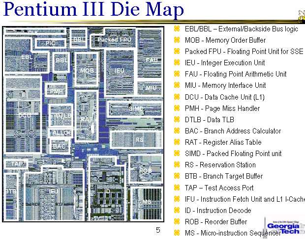
The illustrations above show the P-III functional diagram and the layout of units on a die (CPU variant without L2 Cache). Let's examine some P-III and P-M sub-systems, which seem the most critical for increasing the clock, performance gain, and new functionality. Instruction Prefetch and Branch PredictionBranch prediction performs two main functions — to predict a program address of an instruction to jump and to predict a branching direction (for conditional branch instructions). Both predictions must be done ahead of time — prior to decoding and processing the branch instruction — so that the new block of instructions was fetched without extra clocks or with minimal losses. We shall not review prediction algorithms for branching directions (Intel has accumulated vast experience here). Let's have a look at the Branch Address Prediction and Fast Fetch. This prediction is necessary because this address can be extracted from an x86 instruction and calculated only at the final decode stage, delayed for several clocks. This mechanism is straight-forward in P-III processor, it's based on Branch Target Buffer (BTB) - 512 elements organized like a cache in the form of 128 sets with 4-way associativity. For addressing a set, b10-4 bits of the supposed branch address are used (of its last byte, to be more exact). You can see that a BTB element corresponds to one aligned 16-byte block of instructions — that's the size of prefetch from I-Cache. Thus, there is no need to know the exact address of a branch instruction to make a prediction (it's not yet decoded by that moment) — the prediction can be made by the whole 16-byte block of instructions. This procedure is identical to the one later implemented in AMD K7 (that was mistakenly called "innovative"), but it's more simple as far as algorithm is concerned, without preliminary I-Cache marking and preparation of a selector array. This procedure has the same temporal characteristics as AMD K7/K8, it loses at a branch just one clock, which can be easily hidden even in the tight instruction flow. This procedure allows to predict up to 4 potential branches in the aligned 16-byte block (AMD K8 allows only 3 such branches in a block). Thus, the existing procedure can be recognized as quite satisfactory. Its possible flaw lies in a lot of work per clock (though it's hard to give sharp estimates here). Besides, the new processor may require to increase prefetch to 32 bytes, as 16 bytes may be not enough for 4 instructions (taking into account a possible REX prefix for the new 64-bit instructions and active usage of relatively long SSE instructions). It's also desirable to enlarge BTB from 512 to 2048 or even 4096 elements (like in Pentium 4). There is just a chance that the BTB is already larger in P-M than in P-III. DecoderThe processor contains a "direct" decoder without predecoding instructions prior to putting them into I-Cache (like in AMD K7/K8, for example). Marking (finding the start and the end bytes of instructions) is performed dynamically, at the first clock, right after fetching a block of instructions. Decoding is done in three parallel channels (which will be later referred to as "decoders" for simplicity) according to the asymmetric 4-1-1 scheme: the first decoder can decode instructions, generating up to 4 MOPs, the other two — generating only one MOP. Besides, decoders can work at full speed only with x86 instructions not exceeding 7-8 bytes. These limitations may slow down decoding in some cases to two or one instruction per clock. Strictly speaking, the decode scheme should have been called "4-1-1 / >4", meaning that in case of an instruction generating more than 4 MOPs, only this instruction will be processed. In this case, AMD K7 decoder should be designated as "1-1-1 / >1", as it becomes sequential for a 2-MOP instruction already. We should elaborate here: "1 MOP" in the AMD K7/K8 processors may mean Load-Op. In AMD K8, the decoder becomes "2-2-2 / >2", since it can process all packed SSE and some other 2-MOP instructions in all decode channels. In case of the P-M processor, "1 MOP" may also mean Load-Op and some other instructions with two elementary actions due to micro-op fusion. However, a packed SSE instruction generated two MOPs and thus must be always processed by the first decoder. Besides, SSE instructions like Load-Op are still split into separate Load and Op MOPs and are also processed by the first decoder (packed SSE instructions like Load-Op are split into 4 MOPs). Thus, the P-M decoder, being more flexible in some cases than in AMD K8, has serious limitations in decoding packed SSE instructions and SSE instructions addressing an operand in memory. Besides, it seems too complex to implement, which results in a longer clock and a limited CPU clock frequency. The most complex element in the P-M decoder that makes a principal difference from the AMD K8 decoder is an x86 instruction length decoder. It must mark three incoming instructions prior to sending them to decode channels. Complexity of this instruction length decoder grows, as the number of channels in the new processor is increased to four as well as due to the REX prefix of 64-bit operations and lengthening of the average instruction. We can assume that this chain will be split into several pipeline stages in the Conroe processor. Or there will be introduced an instruction predecode procedure before moving them into I-Cache. Each of these two approaches has its pros and cons. Redesigning decoder in the part where it marks instructions would allow to reduce the volume of work, executed at critical stages of a pipeline, and thus to increase the clock threshold. Does the new processor need a symmetric 4-4-4-4 decoder, or at least a 2-2-2-2 one? It depends on whether there will be changes in the SSE instruction decode scheme and in the organization of generated micro(macro)operations for these instructions as well as in the speed of functional SSE units. If there are no significant changes in this part, the decoder would have to be expanded to "2-2-2-2" or "4-2-2-2" (ideally "4-4-4-4"), in order to provide MOPs for SSE FPU at maximum speed possible (considering the gateway to execution increased to four). However, there is less need for a complex symmetric decoder, if SSE micro-op fusion is introduced in this or that form (for example, if appears a single 128-bit MOP for packed SSE instructions instead of two 64-bit ones). We can assume that the decision will be based on complexity of the decoder scheme and its power consumption. Theoretically, there should be no special problems to implement four "complex" decoders, from the point of view of marking instruction boundaries and their layout. Floating-point arithmetic (x87 and SSE)x87-FPU is currently implemented in P-III/P-M less efficiently than in AMD K7/K8 processors: fmul and fadd instructions are started via a single shared port, fmul is executed at half-rate (but in this sense, x87-FPU is balanced by port and rate for the equal number of addition and multiplication operations). Scalar SSE mode (32-bit SSE1) is rather efficient in P-III: mulss and addss are full-clock instructions and are run from different ports, which provides the total execution rate for such instructions of two per clock. Probably the scalar SSE2 mode (64-bit) is implemented in P-M in the same way. Thus, we have no gripes against FPU for scalar SSE modes. However, the lack of micro-op fusion for scalar SSE instructions like Load-Op introduces limitations at the decode stage and reduces the MOP stream density at other stages. The situation with packed SSE instructions is still worse (see the previous section). Thus, in order to increase performance, SSE requires at least MOP upsizing (connecting two 64-bit operations into one 128-bit operation) for packed instructions. Besides, micro-op fusion for Load-Op is also desirable, or at least expanding a decoder to X-2-2-2, so that such instructions wouldn't slow down the decode rate. The radical performance gain could have been obtained in case of the double-width full-clock 128-bit (2x64) FPU instead of the current single-width 64-bit one. In this case all packed SSE instructions would become single-MOP. This option also requires 128-bit operation of loading XMM-register from memory (cache) — such an operation would be useful, even if the 64-bit FPU is retained. However, the decision will probably be again based on the scheme complexity and power consumption of the new FPU. Execution Ports and Functional UnitsConsidering the quadruple instruction decode and possible expansion of MOPs, the current number of ports (2 universal, 1 Load, 2 Store) and functional units seems insufficient 
At least one more integer execution unit and a corresponding port should be added for executing codes without floating-point arithmetic. In this case we may reach the full (or nearly full) bandwidth proceeding from the "3 integer instructions + 1 Load-Op" scheme. The number of execution ports for floating-point arithmetic is sufficient both in case the current FPU bandwidth is preserved (two 64-bit ports for multiplication and addition instructions correspondingly) and in case the FPU is expanded to 128 bits (FPU remains full-clock). The option with doubling 64-bit FPUs (and increasing the number of FPU ports) looks unpractical. Thus, it's desirable to have three or four ports with possible task sharing and/or overlapping in the new processor instead of the current two universal execution ports. We can assume the following options:
The last option looks the most preferable. However, it requires adding another (the fourth) integer arithmetic unit. Note that the new processor offers 64-bit integer arithmetic, meaning higher complexity of units compared to P-III/P-M processors. There is also an option to add an additional port for 64-bit Load-Op, but expanding the existing port to 128 bits looks a simpler alternative (to load XMM registers). This expansion is necessary in case of the double-width full-clock 128-bit (2x64) FPU instead of the current single-width 64-bit one (due to the doubled necessity of FPU in data). But it may prove useful even if the current 64-bit FPU is retained. CachesInstruction and data caches in P-M processors (32 KB each, 8-way associativity) look quite efficient and sufficient for the new processor. Of course, we'd like to have D-Cache increased to 64 KB. But it would have required increasing the associativity level to 16 (cache indexing by the logical address would have been still required), and an effective design of this scheme may prove to be a difficult task. To increase the data reading rate (especially when the full-clock 128-bit FPU appears), 128-bit reading from cache is desirable, that is the read port should be expanded from 8 to 16 bytes. Two 8-byte read ports are possible instead, as it's implemented in AMD K7/K8 processors — but this option looks more complex. L2 Cache in the P-M processor also looks very good in terms of access times, data rates, and physical density. Theoretically, the current maximum reading bandwidth from L2 Cache (32 bytes per clock) is enough to provide data to both L1 Caches in the dual core configuration (with proper pipelined access). The desktop Conroe processor is supposed to have 4 MB L2 Cache. Introducing Trace Cache for instructions (like in Pentium 4) does not look efficient and justified for this relatively low-clock architecture, as it would have required a full overhaul and a significant complication of the core structure. Prefetch and branch prediction in Intel P-Pro/P-II/P-III/P-M processors as well as predecoding in AMD K7/K8 processors demonstrated that classic instruction caches still had reserved in this sphere — especially considering the simplicity of I-Cache, which is important for reducing power consumption. New prefetch, Fast FSB, Memory, and Access to Neighboring ProcessorsImproved prefetch from memory and advanced memory disambigution will certainly allow to raise reading rates from memory hierarchies and increase calculating performance of "high-bandwidth" programs. Higher FSB clock will also see to that (up to 1066 MHz in Conroe). Shared L2 Cache as well as fast access to L1 Cache of the other processor will allow higher execution efficiency of interacting processes. It may give a powerful incentive to the development of parallelism in desktop applications. Merom/Conroe processors stand out in such features against the current dual core modifications of AMD K8 X2. SummarySo, we seem to have underestimated Intel P6 microarchitecture — especially considering its development in P-III and (in the highest degree) P-M processors. Of course, it's still not perfect enough for tomorrow's requirements. But it can be used as a basis for a new or deeply modified architecture, which would demonstrate good performance results and low power consumption. Addendum: a Little of Gossip :)In conclusion we publish amazing information from the article "Intel Merom is designed from the ground up" (The Inquirer, 23.08.2005). Here are several extracts from the article concerning the new processor:
In this case it might mean, for example, two 64-bit full-clock FMAs (one for each FPU execution port) with total peak FPU performance of quadruple clock frequency (versus the doubled clock frequency in P-III/P-M processors). Doubling the width of the full-clock FPU to 128 bit besides the above said is unlikely, as it would have caused excessive complexity and imbalance of a processor. This option requires either increased reading rates from L1 Cache, or two 64-bit reading ports, or an expansion of the existing port to 128 bits. In the last case, a good balance between load rates and instruction execution speed may be reached only with packed SSE instructions. Theoretically, the fusion of multiplication and addition instructions might be accompanied by the fusion of two operations of a packed (macro)instruction into a single MOP and/or by the fusion of Load-Op (macro)instruction. On the whole, this information does not seem quite credible, this scheme looks unlikely. Creating two full-clock 64-bit FMAs instead of the existing FPmul and FPadd units would require to add addition schemes to the first unit and multiplication schemes - to the second. The multiplication unit is the most expensive here. But on the other hand, this option would be simpler and more economic than full-clock doubled (128-bit) FPmul and FPadd units — with all that in mind, it would allow the same peak FPU performance, without being too much inferior in "irregular" operations (in a number of cases even outperforming it — for example, in case of scalar SSE instructions). The fusion of multiplication and addition instructions into a FMA macro-op poses another problem. Usually after a multiplication, the result with a long mantissa is immediately, without preliminary rounding, added to the operand. It allows to execute a combined operation in the most efficient way. Unfortunately, such an optimization is impossible in our case, as you cannot be sure that a neighboring pair of multiplication and addition instructions will always fuse into a single MOP, when executed dynamically (the process may be prevented by interrupts or other circumstances). As the lack of determinism in binary code execution is inadmissible, we'll have to always round the multiplication result, which will lead to one clock lost at the minimum. However, this requirement does not interfere with the efficient FMA operation in the new processor. Drawing the bottom line, we can say that the information from The Inquirer requires additional confirmations. Let's hope that it will be confirmed — but we shouldn't trust it so far... Conroe Performance TestsThe reviewed architectural peculiarities of the new processor can be divided into two groups: those that allow to raise the clock and those that directly boost the performance. It's hard to give a quantitative evaluation of the first group. So we can only hope that the CPU clock threshold will grow (even if not radically) and rely on the articles. According to them, Conroe clock frequency, manufactured by the 65nm process technology, may reach 3 GHz. Considering the 1066 MHz FSB and 4 MB L2 Cache, let's analyze the CPU performance from several angles:
ConclusionSo, Intel seems to take the challenge of time, "trod on its throat", and designed processor architecture intended "not to set the Thames on fire", but to satisfy users' needs. Exactly in the way the users (and Intel, copying them) imagine it. Now Intel and its processors will be hard to reproach with performance loss in heavy games, with high power consumption and heat dissipation, with the lack of competing dual core solutions, with unjustified passion for technologies of tomorrow. Of course, the public will soon find another reason for unfair criticism. However we must admit that Intel struck back its opponent with its own style and offered products with good characteristics in all "advantageous" (for its competitor) directions. Moreover: if the results of the above analysis are correct, we'll have to admit that Intel will get advantage in most characteristics (probably, except for floating-point performance). It means that the competition must become more sensitive. AMD will have to get out of its "design hibernation" to offer back decent solutions. That will play directly in our hands. Of course, it's a pity that NetBurst will start leaving desktop computers in a year. This architecture appeared ahead of its time. And unfortunately, it was not evaluated fairly. If we call in the aid of our usual Russian analogies, we can say that our roads failed us once again. But the roads (to be more exact, software quality) will not always be so bad. Sooner or later the interest to high-clock long-pipeline architectures will return. We have been seeing the battle between "thick low-clock" and "thin high-clock" architectures for some time already — the entire history of RISC processors is full of such examples. What's more important is that architectures haven't stopped in their development. After the clock frequency threshold was reached, we had an impression that Intel and AMD struck a contract and decided not to modify seriously their architectures any more. Indeed, micro processing technologies are "overforced", it's quite possible to make a pause in their development. Fortunately, it didn't happen — let's hope it won't happen in future either. Especially as there are still reserves (such as speculative decoding of instructions along several directions). Who knows, may be electronic technology will have a break through for us to see the clock frequency growth again? Our life will become more interesting then. So, let's hope that our brave and optimistic assumptions will be backed up, while cowardly and pessimistic ones will not be confirmed. Let's wish good luck to AMD as well. As a result, we shall all be all right :). References
Oleg Bessonov (bess@ipmnet.ru)
September 9, 2005. Write a comment below. No registration needed!
|
Platform · Video · Multimedia · Mobile · Other || About us & Privacy policy · Twitter · Facebook Copyright © Byrds Research & Publishing, Ltd., 1997–2011. All rights reserved. |


