 |
||
|
||
| ||
|
||
|
||
| ||
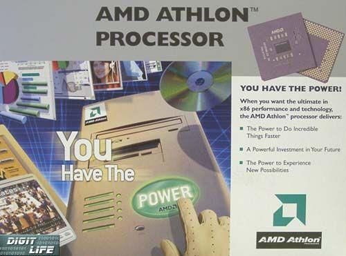
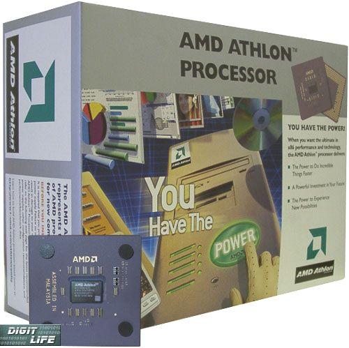
CPU AMD Athlon 1.2 GHz vs Pentium 4 and Pentium
III
 At last you can read a review which will dot all "i's" and cross all "t's" in the opposition of the latest processors and chipsets. On our site you could read a lot of information on CPU Intel Pentium 4 (ASUS P4T, Gigabyte 8TX, Pentium 4) and the only thing left to do is to compare it with its competitors. As for AMD processors we paid not so much attention to it, so you can assume that the review is mainly devoted to the AMD Athlon 1.2 GHz and DDR-chipsets for it. Today we have: Intel Pentium 4 1.5 GHz, Intel Pentium III 1 GHz and two AMD Athlon 1.2 GHz intended for 200 MHz and 266 MHz bus - processors which are on the top of their series and which are more or less acceptable. Note that top-versions of Intel CPU are much more widespread than Athlon 1.2 GHz, especially for 133 MHz bus. We used a set of tests based on real applications. Usage of synthetical tests like Sandra is useless since they show peak unreal 50% superiority of DDR memory over SDRAM For details apply here. In fact, the only wider bandwidth would not help. Let's consider a situation having taken the following question: "Why a system on the KT133A chipset plus CPU Athlon with 266 MHz bus proved to be faster than the same system with 200 MHz bus - of course, with PC133 SDRAM?" The 200 MHz and 266 MHz EV-6 bus on the part "processor-chipset" provides higher bandwidth than 133 MHz part "chipset-memory" with usage of 133 MHz SDRAM. A term "bandwidth", however, refer to data and doesn't characterize the system's performance. Let's consider the following example. While reading or recording a data block into the memory it becomes necessary to output a series of control signals and an address (for the operation to be implemented); it causes a definite delay of the operation with data. But in case of a CPU working on 200 MHz bus, all control signals and the address are transferred at 100 MHz, and the chipset plays a coordinating role taking all 100 MHz signals and converting them for the 133 MHz memory bus. And due to the definite time of non-harmonization of 100 MHz bus "processor-chipset" and 133 MHz data transfer channel, as well as delays in signals proceeding in a matching logic of the chipset, some clocks work uselessly; it causes decrease in efficiency of interaction with memory. And advantage of the 266 MHz EV-6 bus as compared with the 200 MHz one lies not in the higher bandwidth but in the fact that addresses and control signals are given out at 133 MHz what allows to interact effectively with 133 MHz SDRAM. If signals proceed into the chipset and are outputted at the same frequency (i815E and VIA Apollo Pro133A) realization of interaction of memory and CPU can be different. It results in a difference of performance of the systems based on these chipsets. Creation of an efficient memory controller is probably the hardest task. One of the methods is a conveyorization of address signal streams and data streams. It is successfully realized in the i850 chipset. Another method (i440BX) is a synchronous method of organization memory controller where "processor-chipset" and "chipset-memory" part can operate at the same frequency, delays are optimized. Such chipsets provide the max performance as compared with competitors. It seems that it is a desire to create a chipset with an effective memory controller that dictated only partial asynchronism in the i815E as compared with the VIA Apollo Pro133A, the performance, though, turned to be higher. Everybody waited for the AMD-760 based mainboards. This chipset can entirely reveal the potential which promises an interaction of the new CPU AMD Athlon 1.2 GHz intended for 266 MHz EV-6 bus which has 2.1 Gbps bandwidth and 266 MHz PC2100 DDR-memory with the same bandwidth allowing to reach ideally balanced synchronous system. It's obvious that it is exactly the AMD-760 that will set performance limit, which will serve a guiding point for the third chipset manufacturers - ALi, VIA, SiS etc. when producing new revisions of their DDR-chipset and improved drivers for them. Difference in performance among the i815E and VIA Apollo Pro133A chipset is very tiny as compared with a performance range shown by DDR-chipsets, especially now, when chipset and motherboard manufacturers are debugging drivers and BIOS's for their products. Nevertheless, I can't say that now they have raw products the parameters of which will greatly change in the future - a general picture which will be obtained in this testing will allow to consider a potential of each product. Performance results shown by the system on Pentium 4 based on the i850 have reached nearly the max level, and new BIOS versions or drivers will hardly change the situation. This platform, however, can be considered a finished product which doesn't yield to the i815E based systems in stability. And for boards on the DDR-chipsets it is still too early to fight vs the KT133A. The processors differ only in bus frequency and a multiplier. The first one is intended for FSB 100 MHz and multiplier 12, it has Ordering Part Number - A1200AMS3B, and the second one is intended for FSB 133 MHz and multiplier 9 - A1200AMS3C.
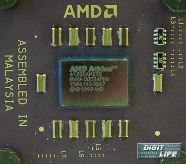
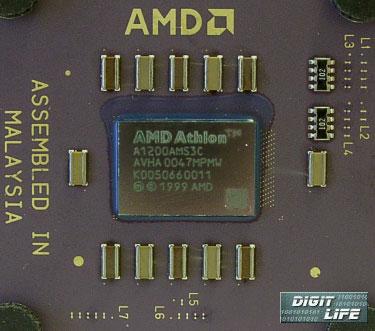 The last letter defines CPU bus frequency. Note that L1 bridges are locked in the both CPUs. The CPU Athlon 1.2 GHz on 133 bus was in a unique box.
 And the last thing to say here. Due to Double-Data-Rate FSB the advantage of CPU Athlon with DDR memory is more obvious than in case of the Pentium III, when 133 MHz FSB "processor-chipset" is a bottleneck. And according to this fact, a demand for the KT266 chipset must be much higher than for the Apollo Pro266. But despite it the Pro266 was first to release boards on which are already available, and the KT266 is in delay. Intel and AMD announced the number of sold processor during the last year. The results are very similar. The number of Intel processors is 4 times higher than of AMD, that's why a market for the Pro266 chipset is wider than for the KT266. The Pentium III is tightly tied up with its 133 MHz FSB, and nobody expects a revolutionary performance gain in DDR systems based on this chipset. It looks like an image product. With its performance it's the fastest and the most functional chipset for the Socket-370 processors. The performance of the KT266 must correspond to the level of the AMD-760, and debugging of the processor bus controllers is going on at full speed. Now let's turn to consideration of the AMD-760 chipset. AMD-760 chipset
 AMD is not aimed at earning money at the expense of their chipsets; they count on their partners, and mainly on VIA. For AMD the new chipset is just a testing area for new technologies and a reserve variant in case of delays in release of chipsets from the third manufacturers. It's proved by cool attitude of the company to development and application of new technologies in case of south bridge production. As a rule, manufacturers prefer to use a more functional south bridge from VIA. Now, before we continue, let me remind you one story: "The processor Atlon with K7 core debuted on the market in August 1999 with 500, 550 and 600 MHz, and by March 2000 they managed to lift the frequency more than 1 GHz. However, after the triumphal 700 MHz CPU whose 512 KBytes L2 cache worked at the max (for Athlon) frequency in 350 MHz, each following Athlon has an increased by 50 MHz frequency but it gave less performance gain. What's the reason? It's simple - they stepped aside from the principle that L2 cache speed was 1/2 core frequency. It is difficult to find cache chips working at the frequency higher than 350 MHz. After that we saw 750, 800 and 850 MHz processors with cache speed from 300 to 340 MHz. After that there came 900, 950 MHz and 1 GHz monsters with the cache working at 1/3 core speed what was equal to 300 - 333 MHz..." To continue the story I should notice that now you can see a similar picture in the difference between memory speed and CPU frequency, e.g. for the 1.2 GHz Athlon and PC133 SDRAM it reached 9 times. The problem lies in the fact that inability of timely provision of the CPU with data has poured from the cache to the main memory. And only AnandTech noticed this, among all famous sites. If the memory hadn't a hierarchical structure, 9 times difference would have been fatal for the CPU. But the situation is remedied by L1 and L2 caches. To be more exact, I should say that comparison of memory and CPU frequencies is wrong - in fact this difference lies exactly in memory and CPU L2 cache frequency where it makes 9 times. With increase in CPU frequency, and, therefore, L2 cache speed the performance gain will be limited by a slow memory. And the lower L2 cache size is, the higher meaning for the performance the speed of the main RAM takes. That's why Duron and Celeron gained more with increase in SDRAM frequency or when migrating to DDR-memory than, for example, Athlon and Pentium III. An ideal variant is increase in SDRAM clock speed, when delay time for all signals is decreasing - control, address and data ones. But how much it will be? It will be significantly cheaper to twice compact only data with minimal reconstructions and keeping the base frequency as it is. This temporary measure will allow processors to increase their frequency for some time not facing deep problems with shipping data for L2-cache. But the price for DDR memory is too high. So, chipset manufacturers started working out products for a new memory type - DDR SDRAM. Intel is saving its Pentium 4, having developed even higher frequencies, with 400 MHz two-channel RDRAM. But Intel is still keeping an eye on DDR. PC133 SDRAM will become used only for entry-level systems. We are waiting for landslide of prices for DDR-memory - the Taiwanese manufacturers have already announced a start of mass production of DDR memory chips. Let's continue to consider AMD-760 chipset.
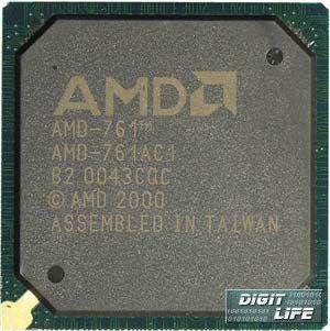
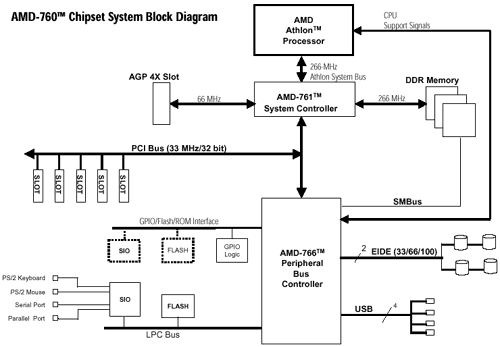 So, the AMD-760 chipset consists of AMD-761 System Controller north bridge, in 569-pin PBGA case and AMD-766 Peripheral Bus Controller south bridge in 272-pin PBGA case. The AMD-761 north bridge consists of a system bus controller of the CPU Athlon, memory controller, AGP controller and PCI. The north bridge supports up to 2 GBytes both PC1600 and PC2100 DDR-memory in case of a usual DDR SDRAM, and up to 4 GBytes in case of Registered DDR memory modules. It's explained by the fact that for usual PC1600 and PC2100 DDR-memory the north bridge supports only two slots. The Registered DDR memory can be installed in 4 slots, what gives 4 GBytes in case of the modules of the max size. Besides, there is ECC support included as well. Together with 200 MHz FSB the chipset supports 266 MHz system bus, processors of which start from 1 GHz. And chipset allows a synchronous interacting of the memory and the processor - with a CPU with 200 MHz bus it is possible to use memory only as PC1600, even if it is PC2100; with the PC1600 memory the processor won't work with 266 MHz bus. And since the boards with a changing multiplier for Athlon processors are not rear, and you can set the lower multiplier and make the CPU work at the same frequency as before but with 266 MHz bus, a purchase of the PC1600 DDR-memory which is not capable of operating at 266 MHz will cause a fall in the overall performance. Development of an asynchronous chipset for DDR-memory is not an insuperable problem. The matter is that delays of signals for synchronization and inevitable influence of any 200 MHz bus on the bus performance "processor-memory" are so high that usage of 266 MHz bus on either part doesn't give a gain relatively to 200 MHz synchronous mode, that's why it was decided to refuse asynchronous modes. Another reason for chipset synchronism is Super Bypass technology, which means that the chipset becomes absolutely transparent for signals and doesn't bring in any delays in their propagation. Usage of Super Bypass is possible only with a synchronous operation of processor and memory buses- by the way, it was used on the AMD-750 as well.
 Unlike other DDR-chipsets, e.g. Ali MAGiK 1 or VIA Apollo Pro266, the AMD-760 supports only DDR memory. The AMD-761 north bridge turned out to be very good. The system bus controller has got a support of 266 MHz bus, the memory controller works with DDR-memory at 200 MHz (PC1600) or 266 MHz (PC2100), and AGP 4x support. The only drawback is that the AMD engineers left only a usual PCI bus. It can be that PCI bus with 133 mbps bandwidth will cope with the load provided by the AMD-766 south bridge. But south bridges of the new series from VIA, shipped together with DDR chipsets and which have a lot of new functions, won't be able to work together with the AMD-761. They are intended for the V-Link bus which provides 266 mbps bandwidth. So, the 686B south bridge turns to be a the best purchase for a user. I hope that in the next chipset from AMD the bridges will be locked by a revolutionary LDT bus which will allow to integrate USB 2.0, Serial ATA in the south bridge without being a bottleneck. Especially considering that in the Crush from Nvidia its usage is already planned. Now you can look at the comparison table of the tested DDR chipset:
In our lab we have tested two boards on the AMD-760 and the both use a tandem AMD-761 + VIA 686B. Of course, they are ASUS A7M266 and Gigabyte 7DX. BoardLet's check the boards' specification now.
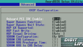
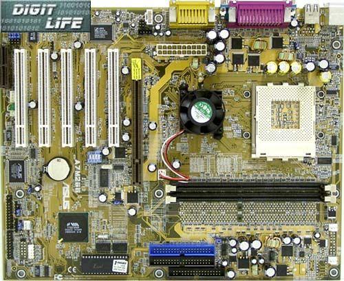 A complete set of the ASUS mainboard includes: a standard red box with a writing "Motherboard Manufacturer N1", the ASUS A7M266 board, a bracket with two additional USB ports and USB, FDD cables, 40-thread and 80-thread IDE cables. It lacks only for a User's Manual. A CD represents a usual CD-R disc. Note that mainboard manufacturers are not able to bring near a price for the boards on the DDR chipset for the price based on, for example, the KT133A. And therefore they tend to compensate high price of them at the expense of cheap additional controllers for realization of external IDE RAID, more or less full-value sound etc. Let's see what the ASUS board is equipped with. It has a full value 4.1 sound from C3D on the CMI8738 chip. There is a space for a network controller form 3Com 3C920 - it will definitely be installed on the next revisions of this board. There is AGP Pro slot allowing to use video cards with increased power consumption. There is not only a heatsink, you can find also a fan. Unfortunately, there is no possibility to change a multiplier. There is space for DIP-switches, and they will probably appear in the nearest future. The board is equipped with 4 switch units - one is responsible for FSB frequencies, the second one works with core voltage, the third one sets memory voltage, and the last one sets the chipset voltage. The first two are doubled into BIOS, which is based on the Award Medallion BIOS v.6.0. Here you can adjust memory functioning, set interrupts to PCI slots and setup AGP operating modes - in other respects it is a standard BIOS from Asustek, which has, as usual, quite a lot of settings of the system. You can change FSB frequency in the BIOS from 100 to 180 MHz, but it is implemented inconvenient - you can add or substract the frequency only by one 1 MHz.
 The Gigabyte complete set includes the Gigabyte 7DX board, a set of FDD cables, 40- and 80-thread IDE cables and a CD. It lacks only for a User's Manual. Gigabyte integrated a cheap sound solution on the base of the CT5880 chip from Creative, which like the C-Media solution allows connecting 5-speaker audio systems. The board is equipped with a cooler for the chipset which is stuck with some transparent substance whose heat-conducting properties are doubtful. By the way, the ASUS has the same thing. The AGP slot is equipped with a clamp for cards, what is sometimes quite useful. The Suspend to RAM function is realized with a jumper on the motherboard (in the manual you can read in details what you should do in that case). Another peculiar feature of the Gigabyte 7DX board is the way of realization of the unbuffered support, or registered memory modules - it is again made in a jumper on the mainboard. The board features a unit of DIP-switches responsible for FSB frequencies - 95, 100.7, 100.9, 103, 105, 110, 115, 133 MHz; note that this function is not doubled in the BIOS, and frequency setup can be implemented with either jumpers or with the proprietary utility from Gigabyte - EasyTune III. Nevertheless, in the BIOS you can find memory settings which are even richer than in the A7M266 board from ASUS. In the Gigabyte 7DX you can't change voltage supplied to the chipset and the memory. And there is no possibility of changing a multiplier, like in the Asus board. But unlike in the case of the Asus I don't see any ways of implementing such solution in further versions. PerformanceThe following hardware participated in our testing: CPU Intel Pentium 4, which has only one platform at its disposal - the i850 chipset and with RDRAM memory. CPU Intel Pentium III, which has only two platforms at its disposal - the i815EP chipset with SDRAM and the VIA Apollo Pro266 with DDR SDRAM. CPU AMD Athlon: here we have four platforms - the VIA KT133A with SDRAM, the AMD-760 with DDR SDRAM, the Ali Magik 1 with SDRAM and the ALi Magik 1 with DDR SDRAM. The last two platforms are introduced in one mainboard which features slots both for SDRAM and for DDR memory. The both boards on the AMD-760 chipset considered in the previous part showed identical results, that's why their results on the diagrams are shown under the chipset's name. In order to eliminate an effect of the video subsystem we used a modern video adapter on the GPU GeForce2 Pro, with 64 MBytes 400 MHz DDR memory. But in the nearest time we are going to assemble testbeds based on the GPU GeForce3 (NV20). All test systems are equipped with 256 MBytes memory what considerably unloads the disc subsystem and minimizes its influence on the platform's performance. This feature allows to reach performance gain around 5-8% in business applications. All mainboards with DDR chipsets are not series samples, that's why we didn't try to reveal their stability characteristics. We were surprised that for some systems business or game benchmarks were difficult to pass. In new revisions of the boards and in new BIOS versions these problems will be solved, and then we can come back to a stability issue. Note that on the AMD-760 based boards the operation failed not only at 266 MHz bus speed but also at 200 MHz with an approx equal periodicity. So, I can say that problems with 266 MHz bus frequency in the AMD-760 are successfully solved and it is mainboard manufacturers that should be blamed. But note that the AMD-760 based samples were received in the last year, and it can be that problems are already smoothed down. The system on the KT133A showed perfect stability both with 200 MHz and 266 MHz CPU versions of the AMD Athlon 1.2 GHz. The following hardware was used for performance estimation:
Software:
Office applications:
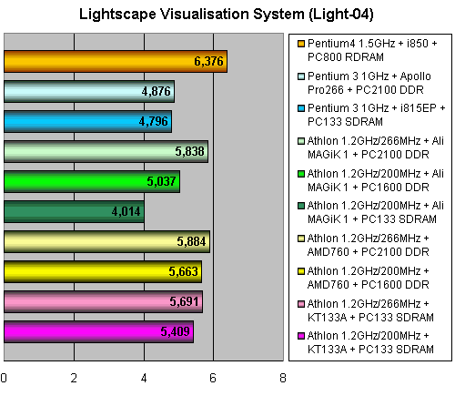
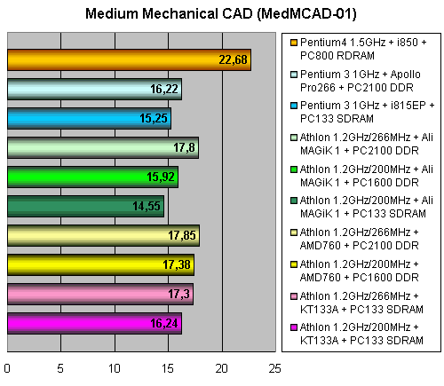
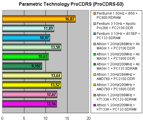
Professional applications:
Games:
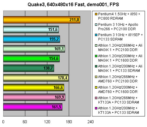
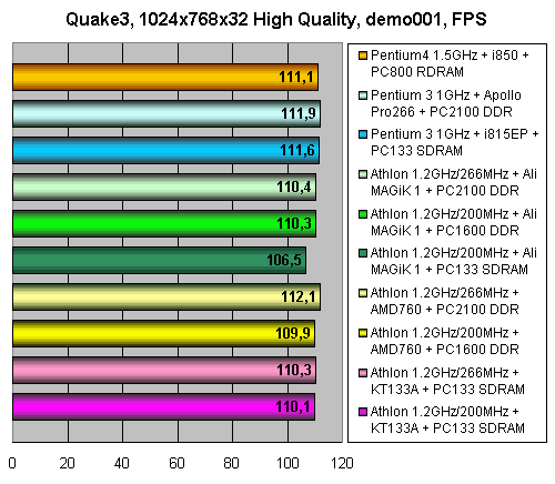
I'll try to explain shortly what influences performance increase in game applications. Note that it's difficult to prove something in the experiments with games whose engines have unclear design. But it's clear that migration to DDR memory for games is undoubtedly a good thing. Multipassage and multitexturing for different light effects and fog, all kinds of shades and flashes, a lot of huge textures. All these will be realized faster with DDR memory, since at the CPU stage a powerful processor will be stand idle waiting for the memory, what is happenning in case of the SDR SDRAM. The less time CPU is idle, the higher the performance is. Scene visualization requires to transfer a huge volume of data from the system memory - textures and coordinates of all vertices, of course under the condition that the HW T&L is not used with local memory data. The FPU calculates lighting of each vertex. Driver and application optimization plays a great role for sets of 3DNow! and SSE instructions. Let's start with Quake 3. It makes the lighting and single-skin via HW T&L, though, that's why even on the GeForce 256 we get 100-120 fps at 1280X1024. Due to the fact that the Quake 3 engine supports hardware transformation of vertex coordinates with the help of the geometrical FPU integrated into the GeForce2 chip, data from the CPU are transferred into GPU. Vertex coordinates are transformed and final geometry stages are implemented - vertex clipping and projection of the screen coordinates into the system. In the Unreal Tournament and Rage Expendable which are using API Direct3D 6.0 the situation is a bit different, since none of the functions of the geometry stage has hardware support in the engines of these games, and all stages are implemented by the CPU. Note that usage of the D3D doesn't cause an impossibility of usage of the HW T&L (starting from DX7 in the D3D the HW T&L is supported). And for the UT they are preparing a patch for operation on the D3D8 with usage not only HW T&L, but also vertex/pixel shaders. On the other hand, a sequence of geometry stage operations (TCL) remains the same. Data are transferred via the busses the same way. The difference lies in the fact that in this case the data volume transferred into a video adapter will be considerably lower. With usage of HW T&L all data are kept in the local memory. We tested in Quake3 with usage of the demo001 at all resolutions from 640 to 1280 and 16 and 32 bit color depth. The UT testing was carried out in 1024x768x32 mode with usage of Reverend's Thunder.dem and UTBench.dem. The first demo is rather simple (two competitors in one room). The second one looks like the Quake3 demo001. The Expendable testing were in two modes - 640X480X16 and 1024X768X32 with usage of the integrated Timedemo.
 [ More results ]
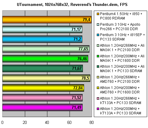
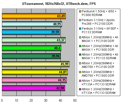
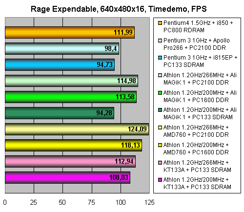
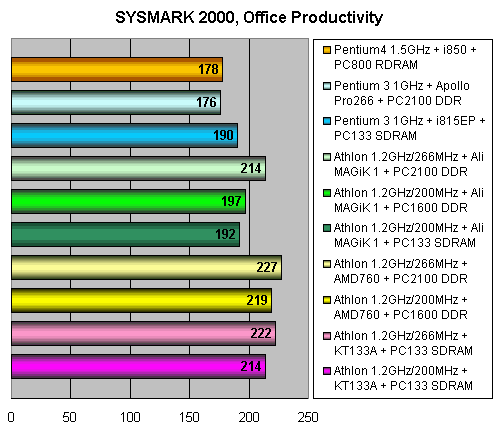
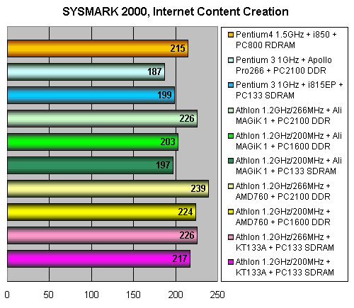
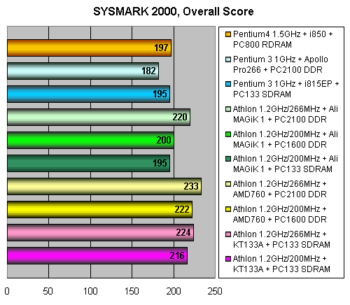
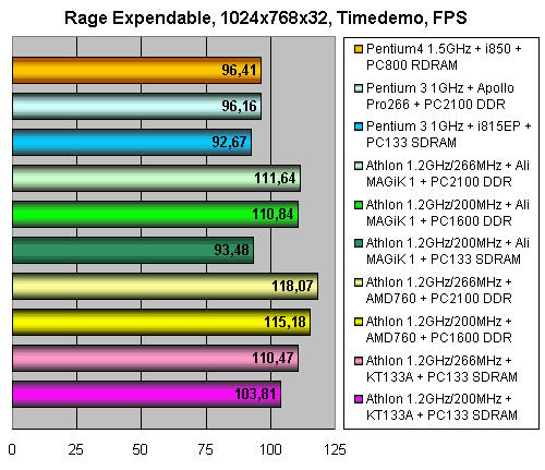 Let's start with the Quake3. The game requires high bandwidth of the "processor-memory" bus and computational resources for figures with floating point at the CPU stage. Quake 3 uses the CPU for different culling schemes. Quake 3 uses huge textures and video memory bus is greatly loaded. The SSE set of operations of the Intel processors is richer than the 3DNow! from AMD, but for Quake 3 the 3DNow! is more than enough. The problems is that normal compiling programs are absent. The developers do not want to deal with code optimization in Assembler. Intel has its own compiler: ICL with support of some calculations. Vectoring is made only on simple operations and with special data organization. That's why developers chose the most convenient SSE set. So, the SSE support is realized in the Quake 3 much better, and the OpenGL driver from NVIDIA is optimized for the both. As a result, a legendary performance of the AMD FPU is graded. Now there SIMD-instruction sets are coming into the fight, as well as buses with high bandwidth and CPU clock speeds. The Pentium 4 looks a favorite. At the expense of the SSE the Pentium III is also ahead. If it is not 200 MHz difference, it could have outperformed the Athlon (KT133A). The Athlon 1.2/266 on the AMD-760 with PC2100 memory performed well - a well balanced system. As for the Apollo Pro266, it can't boast with its results, as well as the ALi Magik 1 chipset. The performance of the ALi Magik 1 with SDRAM memory is disappointing. The KT133A showed good results, but it is maximum it's able of. At 1280X1024 the performance is limited by the fillrate of the video adapter based on the GeForce2 Pro. The situation in the Unreal Tournament is different, what was caused by the peculiar features of the engine in this game. In the UT there are quite a lot of program calculations and they are bad optimized. And the engine's code was adapted for the OpenGL/D3D. Some operations which are fast on the 3dfx+Glide work slow on the OpenGL/D3D + TNTxxx/GeForcexxx. In the Unreal Tournament the culling scheme is rather effective, based on portals. That's why in this game the HW T&L wouldn't have got huge load - everything is done by the CPU. None of the SIMD optimizations doesn't help here. In the Unreal Tournament the load on the "processor-memory" is even higher than in the Quake3, for example, at the expense of palette textures and procedure textures (generated and sent to the card on each frame) - and as a result, the performance changes considerably. Unlike the Quake3, drivers for the UT are no more optimized. The memory bandwidth helped the Pentium 4 and Athlon on the 266 MHz bus with DDR memory on the AMD-760 and ALi Magik 1 to become leaders in the Thunder test. On a more complicated test - UTBench - with a larger number of gamers the FPU performance contributed in the overall performance due to the more complex calculation schemes of collisions among gamers - the Athlon is above all here. The Expendable uses API Direct3D. Being specially optimized for the 3DNow!, it revealed the advantage of the Athlon. Memory load is also large - it's exactly in the Expendable the system on the Pentium III with DDR memory on the Apollo Pro266 managed to outperform the i815 with SDRAM. The Pentium 4 has a reversed set of SSE2 operations. It will allow optimization of a program code for which 32bit SSE/3DNow! real numbers were not very accurate. For example, calculations according to the physical laws, skeletal animation, collision processing. A perfect performance is shown by the AMD-760 chipset; the ALi Magik 1 looks poor, but the both have a potential for performance increase. The DDR-memory is a perfect remedy for enthusiasts of game industry. Now let's turn to business applications. The SYSMARK 2000 consists of two application sets - Office Productivity and Internet Content Creation - which are installed, started up and timed in turn and deleted before installation of the next application. So, the system performance is measured on each application separately. A set of widespread applications is successful and allows a user to estimate whether its system is suitable for one or another operation. The result of each application is given out in scores - the higher, the better. The total score for each set and test is an average value of all scores in each test separately. The Ziff-Davis Media (ZDM) Business Winstone 2001 and Content Creation Winstone 2001 tests supplement the SYSMARK 2000 in the best way - they have a good set of applications for 2001 and run all applications simultaneously, switching between them and delivering their results to each other. As a result, we get a model of a real process of creating of a document or contents. The total operation time of each test is timed and the final result is given out in scores - the higher , the better. A set of the ZDM Business Winstone 2001 tests includes the following applications:
A set of the ZDM Content Creation Winstone 2001 tests includes the following applications:
For performance estimation in business applications there is used one of the most popular resolutions - 1024x768 with 16 bit color depth.
 [ The detailed results are here ]
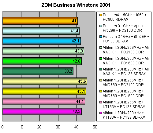
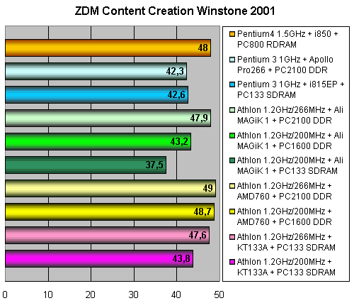 So, the Pentium 4 feels confident in creation of the internet contents fighting with the AMD Athlon as equals, but in business applications it shows moderate results falling behind even the Pentium III. The Pentium III has lost. That's why it will be required only in two cases - for operation in the SSE optimized Photoshop, or at the quite competitive price. By the way, Intel is making some steps putting old models of the Pentium III into the value market. We didn't doubt that the Athlon would win, and migration to the 266 MHz bus and usage of the DDR-memory makes this processor unreachable for competitors in the majority of business applications. But in case of contents creation in the ZDM Content Creation Winstone 2001 at the simultaneous operation of several stream applications, a gap with the Pentium 4 became minimal. For AMD it's necessary to increase frequencies in order to remain a leader. Now we are turning to the professional tests SPECviewperf v6.1.2 and 3DStudio MAX R3.1. All programs of the SPECviewperf v6.1.2 test are very hard Hi-End OpenGL applications and implement mainly a rendering of the complex textures of several hundreds of thousands polygons, with usage of lighting, gradual shading, alpha-channel, edge anti-aliasing. All applications implement rendering in a real-time mode using OpenGL driver. The main difference from games lies, first, in the fact that the structures contain a less number of vertices than the Quake3 or UT levels, that's why the memory bus's load is not so big, but the number of visual and covered polygons in a frame is very big. It means that the overdraw and the fillrate of the graphics accelerator is mainly used for pixel drawing which won't be seen at the end. In the professional OpenGL applications the high frame rate is not required, but it's necessary to provide high accuracy and quality of an image. In games there are a lot of different optimization schemes are used in order the fillrate of the graphics accelerator to be used maximum effectively. We thus have for example 200,000 texture polygons in a frame against 20,000 e.g. in the Quake 3. The load on the bus of the local memory and the CPU, and the frame rate falls down to 20. Only the first test which demonstrated a running person shows an acceptable FPS on the GeForce2 Pro. The first place is shared by the SSE and 3DNow! optimization. All tests showed that the Pentium 4 1.5 GHz outperforms the Pentium III 1 GHz by 1.5 times. The second professional test is the 3DStudio MAX R3.1. In the tests there were two scenes from a set for measurement of the OpenGL video subsystem performance - 4views.max, which is an animation of 90 frames of the turning table with several objects (the number of polygons is 40,000), and geom1.max, which shows a flight of a camera over the landscape of 150 frames (the number of polygons is 200,000).
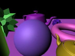
 These screenshots are frames after rendering of the files 4views.max and geom1.max It's obvious that in case of full-value program rendering the FPU carries the whole load, and the Athlon should prove its superior might. In case of usage of the SPECviewperf v6.1.2 and 3Dstudio we used resolutions close to real conditions of designer's working - 1280x1024x32.
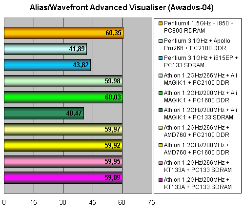
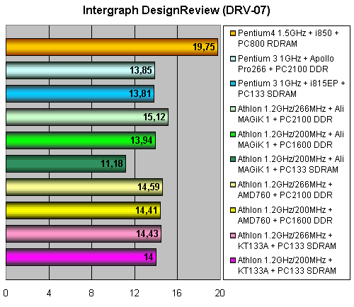
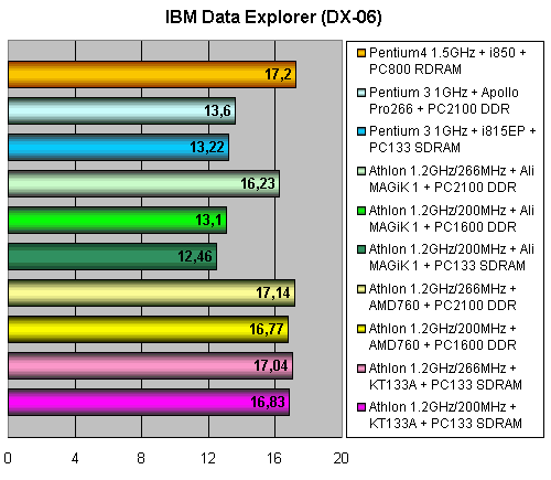
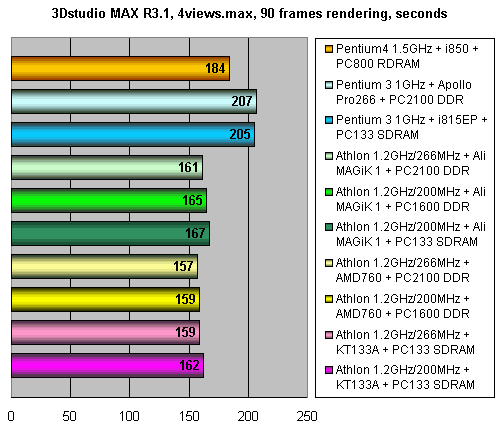
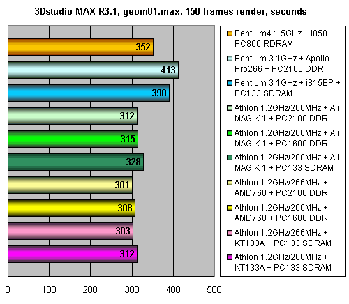 For professional use in 3D modeling systems the Pentium 4 suits the best. But the Athlon keeps the same margin. Performance gain in case of usage of DDR memory and 266 MHz bus is insignificant. In this test the Magik 1 performed very good. By the way, it's nearly the only test where an advantage of the DDR memory over the SDR for the Pentium III is noticeable. I hope that with optimization of drivers and BIOS the Apollo Pro266 will be called for not only due to its wide functionality, but also due to high performance. The last comes the 3Dstudio MAX. The results of the Athlon 1.2 GHz / 266 MHz on the AMD-760 exceeded the Pentium 4 results in the both tests by 17%. That's why if you are making rendering of animation on the professional base, you will need a dual-processor system, and among uniprocessor systems the choice should be made for the Athlon. ConclusionIt's obvious for a usual user, who is engaged in everything a little, one of this processors will be more than enough, and he should make a choice according to his tastes and prices for the system as a whole. If you are a professional dealing with a computer modeling, rendering and math calculations, then you are facing another problem - a maximum system performance mustn't affect reliability and stability. That's why I recommend you systems which use SDRAM - the Athlon with the KT133A and the Pentium III with the i815 or the Apollo Pro 133A, and RDRAM system Pentium 4 on the i850. And as for systems on the DDR chipsets - Ali Magik 1, AMD-760 or VIA Apollo Pro266 - you'd better await. I think that by the end of February we will see debugged commercial board revisions and improved BIOS and drivers. And if prices for DDR memory would fall, then expect a spring boom for DDR The Pentium 4 with RDRAM is cheap enough to become affordable for majority of users Let's see what will be the further way of SDRAM.
Write a comment below. No registration needed!
|
Platform · Video · Multimedia · Mobile · Other || About us & Privacy policy · Twitter · Facebook Copyright © Byrds Research & Publishing, Ltd., 1997–2011. All rights reserved. | |||||||||||||||||||||||||||||||||||||||||||||||||||||||||||||||||||||||||||||||||||||||||||||||||||||||||||||||||||||||||||||


