 |
||
|
||
| ||
|
||
|
||
| ||
"A new generation of Pentium processors. Be ready to meet Intel Pentium 4. Based on a completely new architecture Intel NetBurst, Pentium 4 processor establishes a new standard for high-performance microprocessors. New generation of performance. The processor of a new generation intended for desktop computers features an improved Intel's micro-architecture and a powerful set of additional functions developed to provide an optimal performance for working with the latest Internet-technologies. Get the maximum performance with a new processor Intel Pentium 4 from the leader in microprocessor production..." Part I: the history |
|
Tweet | ||
It's obvious that advertising plays an enormous role in product's promotion. And such a unique product as Pentium 4, which ensures unbelievable performance to everybody, especially to the Internet fans, has to become successful.
Note that the processor, which hasn't been yet debuted, is just like a snowball - it collects incredible number of rumors, different tests both positive and negative, guess-works again believable and preposterous. Well, in this article we will try to look into all this stuff and give a full reliable description of the product, which is what Intel counts on in the nearest 2 years.
The article consists of several nearly independant parts to make it convenient for our readers (you can choose what you are interested in and miss other stuff).
Nobody would doubt that Intel Architecture became a standard of the modern computer industry. The basic factor of such popularity, as Intel considers, is a full compatibility of software, developed for Intel Architecture processors, and great performance increase in new generation processors. Let's follow the development of the company from the very beginning - 16-bit architecture to the modern 32-bit IA-32 architecture which is used in all latest processors from Intel.
The first models of Intel Architecture were 16-bit processors 8088 and 8086, and the object code, developed for them in 1978, is now being implemented in the latest processors of IA-32 architecture.
8086 processor had 16-bit general-purpose registers, 16-bit data bus and 20-bit address bus, what allowed to operate an address space of 1 MBytes. 8088 processor differs only in 8-bit data bus.
These processors brought in a segmentation in IA-32 architecture. The memory was divided into the segments of up to 64 KBytes each. Operating with 4 segment registers simultaneously the processor could address up to 256 KBytes memory without switching between the segments. 20-bit addresses were achieved by adding 16-bit address to the segment register pointer.
An enhancement in 80286 processor for IA-32 architecture was made in form of the protected mode. Within the mode, the contents of the segment registers are used as a pointer to descriptor tables, which gave a possibility of 24-bit addressing, what constituted 16 MBytes of address space. Besides, there appeared a possibility to control segments' borders, read and execute-only options for segments, 4 level protection for the OS code from applications, and protection of applications from each other.
Intel 80386 became the first 32-bit processor in IA-32 architecture. The architecture received 32-bit GP (general purpose) registers, matching both address storing and operands. The lower and upper halves kept the possibility to serve as independent registers to provide compatibility with the previous processors. Then, they brought in a virtual x86 mode to provide an effective code implementation created for earlier processors.
With 32-bit address bus, 80386 processor supported addressing up to 4 GBytes memory. And there you could use both segmented memory and "flat", when all segment registers contained the same address pointer, and in each segment all 4 GBytes address space was accessible. For virtual mode there was announced a page method, when the whole address space is divided into fixed pages maximum of 4 KBytes (it was much more effective than segment processing). 16-bit instructions received a possibility to work with 32-bit operands and addresses. Besides, there appeared a new set of 32-bit instructions.
For higher performance gain in 80386 was realized a parallel work of several processor units, what initiated staging in 80486.
In a new processor 80486 an instruction decoding unit and a calculating unit were transformed into 5-stage pipeline, where each stage could operate together with the others at the same time implementing up to five instructions at different stages. A full processing of each instruction takes some clock cycles; but it's quite convenient to divide the process into several stages when the next instruction starts being operated right after the previous instruction has passed the first stage. This method is an easy way to receive quickly several completed instructions. Then, there came such innovations as 8- KBytes cache of the first level in the chip to provide the thorough loading of the pipeline, an integrated õ87 coprocessor, and support for a cache of the second level.
Pentium became the first one which had got the superscalar architecture - 2 pipelines U and V allowed to implement 2 instructions per clock cycle. L1-cache became twice more: both instructions and data could dispose of 8 KBytes, the data cache utilized more effective scheme with back writing. An integrated branch table was used for branch predictions in cyclic constructions.
In the virtual õ86 mode in addition to 4- KBytes pages there appeared 4 MBytes pages support. The registers remained 32-bit, but some internal buses extended up to 64 and even 128 bits. Besides, the external data bus became 64-bit.
The last processor of that generation, Pentium MMX, brought in an extended set of instructions allowing to operate effectively with packed integer data located in 64-bit MMX registers.
In 1995 P6 series processors were announced with yet 3 independent pipelines. The first one was the Pentium Pro.
The main difference is that P6 converts x86 instructions into internal, RISC-like instructions called micro-ops. It allows to avoid many limitations which are peculiar to x86 instructions, such as irregularity of coding, operations of integer transfers "register-memory" and variable length of immediate operands.
The address bus extended to 36 bits, what allowed using address space of 64 GBytes.
Pentium III brought in in IA-32 architecture SSE extensions (Streaming SIMD (Single Instruction Multiple Data) Extensions) - there became available new 128-bit registers and SIMD operations on packed operands with floating point with single precision.
|
Processor |
Release date |
Frequency (when released) |
Transistors |
Register bit capacity |
Data bus bit capacity |
Address space size |
Cache size |
|
8086 |
1978 |
8 MHz |
29 K |
16-bit general purpose registers (GP) |
16 |
1 MBytes |
- |
|
80286 |
1982 |
12,5 MHz |
134 K |
16-bit GP |
16 |
16 MBytes |
- |
|
80386DX |
1985 |
20 MHz |
275 K |
32-bit GP |
32 |
4 GBytes |
- |
|
80486DX |
1989 |
25 MHz |
1,2 M |
32-bit GP, 80-bit FPU |
32 |
4 GBytes |
8 KBytes |
|
Pentium |
1993 |
60 MHz |
3,1 M |
32-bit GP, 80-bit FPU |
64 |
4 GBytes |
16 KBytes |
|
Pentium Pro |
1995 |
150 MHz |
5,5 M |
32-bit GP, 80-bit FPU |
64 |
64 GBytes |
16 KBytes L1; 256, 512, 1 K L2 |
|
Pentium II |
1997 |
266 MHz |
7 M |
32-bit GP, 80-bit FPU, 64-bit MMX |
64 |
64 GBytes |
32 KBytes L1; 256, 512 KBytes L2 |
|
Pentium III |
1999 |
500 MHz |
8,2 M |
32-bit GP, 80-bit FPU, 64-bit MMX, 128-bit XMM |
64 |
64 GBytes |
32 KBytes L1; 256, 512 KBytes L2 |
Before considering the architecture of a new processor from Intel - Pentium 4 Willamette, and comparing all the enhancements brought in with up-to-date processors, I'd like you to pay close attention to P6 series architecture - all Intel processors of to-day belong to its series.
A full processing of each instruction takes a definite number of CPU clock cycles. Here it's possible to divide the process into several stages, what will let to start the next instruction implementation right after the first instruction passes the first stage - this is what we call a pipelining, which took place in the days of 80486 processors and Pentium, where a standard 5-stage pipeline is used.
Superpipelining, which is applied to P6 series, divides the stages into smaller parts. Apparently, the smaller stage implements less work, and therefore, contains less hardware logic. The time interval between input actions set, entering the scheme input, and appearing of resulting signals on the scheme output is called a propagation delay. Here it becomes significantly less, what allows... Attention!
Thanks to shorter propagation delays of the signal in each separate pipeline stage, it's possible to increase the clock frequency.
A similar effect of decreasing propagation delays can be achieved with the usage of a new technology - i.e. .13 instead of .18 micron.
It's obvious, that P6 series architecture, used in P3 processors, became exhausted with the frequency a little more than 1 GHz as for .18 micron technological process.
Superpipelining features one serious drawback. When implementing mispredicted branches and operations, there is needed a complete clearing of the pipeline, and the more stages, the more time this clearing takes. Sometimes, there can be a considerable performance decrease.
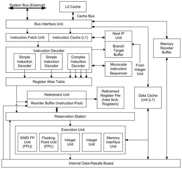
Let's consider stepwise work of P6 processor's pipeline which consists of 12 stages. The pipeline can be divided into 3 independant functional units: in-order front end which controls instruction decoding and processing, out-of-order core where the instructions are executed, and in-order retirement pipeline.
Instruction fetch unit reads an instruction flow from L1-cache of instructions at 32 bytes per clock cycle. In order to find the beginning of the instruction there used a current IP-instruction pointer, and then, aligned 16 bytes of an instruction are transferred to 3 decoders. In case an instruction is located in the end of the first line of the cache, the second line is read also to receive missing bytes.
Before we take a leap to decoder work, let's consider the mechanism of branch prediction.
IP-instruction pointer is calculated by the instruction fetch unit on the base of the information from BTB (branch target buffer) and based on the branch history bits, which are generated by the Integer Unit.
Transition (branch) prediction is intended to minimize an idle work of the pipeline and provide it with the continuos instruction flow. On average, unconditional branches constitute up to 10 % of the program code (they transfer the control to the new indicated address), and conditional transfers constitute 10-20 % (they change or not the direction of an instruction implementation depending on the result of comparing or some other conditions). If the conditional transfer can't finish, the program passes to the next instruction.
Unconditional branches do not cause any problems; the processor knows exactly that they will be done, and it starts instruction fetch according to the indicated address. Conditional branch instructions can cause some difficulty, since the processor doesn't know whether they will be implemented until they pass an executive pipeline stage. But the suspense until the instruction doesn't leave an executive stage means a temporary failure in fetching and processing following instructions.
To predict a branch, the processor utilizes an extended algorithm of Yeh. If the prediction is true, the implementation will be continued with a little delay or even without it. If it's not, the partly done instructions have to be deleted and new instructions with the right address must be chosen in the memory, decoded and implemented. It brings about a significant performance decrease which depends on the pipeline depth (for P6 architecture the losses can reach up to 15 clock cycles).
Branch prediction algorithm is dynamic, 2-level, and based on the behavior of the branch instructions during the previous time interval (since the same jump can be implemented more than one time, i.e. in a cycle), and on the behavior of definite groups of instructions, for which there may be predicted a definite jump quite exactly. Prediction accuracy of the given algorithm constitutes appr. 90%.
So, aligned 16 byte instructions are transferred into Instruction Decoder which consists of 3 parallel decoders, 2 of them are Simple and the last one is Complex. The task of each decoder is to convert IA instruction into one or more micro-ops.
Simple decoders process x86 instructions which are translated into a single micro-op. A Complex decoder works with the instructions which correspond to 1-4 micro-ops. If an instruction is too complicated even for the complex decoder, it is transferred into MIS (microcode instruction sequencer) which generates the necessary number of micro-ops. If a Simple decoder receives a complicated instruction, the latter goes to a Complex decoder, or even to MIS. This slows decoding, but thanks to buffering with Reservation Station it doesn't effect the performance strongly.
If simple and complex instructions are implemented by the corresponding decoders, these decoders can generate 6 micro-ops at a clock cycle, but as a rule, there are only as much as 3 micro-ops that correspond on average to 2-3 IA instructions which are transferred into ROB (Reorder Buffer). ROB contains 40 elements of 254 B each, and can store a micro-op, 2 operands connected to the micro-op, the result and some status bits.
The last stage before instruction implementation is register renaming which is carried out in the RAT (register alias table). x86 architecture provides only 8 32-bit general purpose registers, and the probability that 2 neighbor instructions will use the same register is relatively high. Register renaming helps to weaken an influence of such register dependencies - in case of necessity to write both instructions in the same register, it will be impossible to implement them out of turn without register renaming, since the following op can't be processed until the preceding op is done.
With register renaming the program references to architectural registers are converted into the references to 40 physical registers of micro-ops which are realized in the Reorder Buffer. Essentially, the processor makes clones of the limited number of programmable architectural registers and traces what clones contain the latest values.
Reservation Station serves as an executive program and microcode instruction sequencer, for what the Station scans the reorder buffer continuously and chooses the instructions ready to be processed (with all initial operands). The result goes back to the buffer and is stored there together with micro-op until output. Instruction processing order is based on the fact whether the instruction and its operands are ready to be implemented (and not on the initial sequence), this is what is called "out-of-order".
If the decoders stopped working, the executive units continue to work using the instructions from the Reservation Station, and in case of the executive units are in busy condition, the Reservation Station allows the decoders to work. When the Station is being filled (though it's quite rare), there is some suspense in work of decoders.
The micro-ops are implemented with the help of two integer units, two floating point units and one memory interface unit - therefore, it's possible to implement up to 5 micro-ops at a CPU clock cycle.
Two integer units are able to carry out 2 integer micro-ops at the same time. One of the units is developed for branch operations. It's able to reveal a branch misprediction and to notify the branch prediction buffer of need in pipeline restart. Let's consider the detailed process.
The decoder attaches the both addresses to the branch instruction: the predicted branch address and the one previously declared invalid. When the integer unit executes a branch operation, it can define what branch was chosen. In case of the predicted branch, all cumulative and executed instructions of this branch are marked as disposable for further use, and there goes on further implementation of this branch. Otherwise, all instructions of this branch are considered as "withdrawable". Then, the address buffer receives the right branch address and restarts the pipeline from this address.
Memory interface unit is charged with loading and storing micro-ops implementation. The loading requires only the memory address, that's why it can be represented with one micro-instruction. The storing requires also what to be stored, therefore it's coded with 2 micro-instructions. A part of the unit that processes instructions of storing has two ports, what allows to process an address instruction and data micro-instruction simultaneously. Then, loading and storing instructions can to be covered also at a clock cycle.
There are 2 units for floating point operations (the second one is intended for SIMD instruction processing).
Instructions, which are processed in the order different from the established by the program (speculative), are to be put in the right order, or the processor will be never able to receive right results.
The reorder buffer keeps the status of execution and stores each micro-op results. The micro-op is output with the Output Unit. The latter scans the reorder buffer for micro-ops, which mustn't influence the implementation of other micro-ops.
Such instructions are considered completed, and the output unit forms of them the initial sequence, counting interruptions, exclusions, breakpoints and branch mispredictions.
The output unit is able to output 3 micro-ops at a clock cycle. With the output of a micro-op, the results are recorded into RRF (retire register file) or/and memory. RRF contains 8 general purpose registers and 8 registers for floating point data. As soon as the micro-op is output, it's deleted from the reorder buffer.
Operations of record into the memory are postponed until the micro-op that called them is output. For it P6 contains MOB (memory order buffer), where the information on data and addresses of instructions, given by the record unit to the memory, is kept. The MOB sends the data to the memory only after the reorder buffer notifies the former that the micro-op, which made a record in the memory, is deleted.
Well, we have considered the basic principles of work and layout of P6 series processors. We'll trace the difference between Willamette - Pentium4 (developed from "zero"), the minimum clock frequency of each is 1.4 GHz. Is it a really breakthrough or just a way to overcome the cutoff of the crystal within 0.18 micron technology?
The answers to these and many other questions will
be given in the next part of our review...
Write a comment below. No registration needed!
|
Article navigation: |
| blog comments powered by Disqus |
| Most Popular Reviews | More RSS |
 |
Comparing old, cheap solutions from AMD with new, budget offerings from Intel.
February 1, 2013 · Processor Roundups |
 |
Inno3D GeForce GTX 670 iChill, Inno3D GeForce GTX 660 Ti Graphics Cards A couple of mid-range adapters with original cooling systems.
January 30, 2013 · Video cards: NVIDIA GPUs |
 |
Creative Sound Blaster X-Fi Surround 5.1 An external X-Fi solution in tests.
September 9, 2008 · Sound Cards |
 |
The first worthwhile Piledriver CPU.
September 11, 2012 · Processors: AMD |
 |
Consumed Power, Energy Consumption: Ivy Bridge vs. Sandy Bridge Trying out the new method.
September 18, 2012 · Processors: Intel |
| Latest Reviews | More RSS |
 |
Retested all graphics cards with the new drivers.
Oct 18, 2013 · 3Digests
|
|
Added new benchmarks: BioShock Infinite and Metro: Last Light.
Sep 06, 2013 · 3Digests
|
|
Added the test results of NVIDIA GeForce GTX 760 and AMD Radeon HD 7730.
Aug 05, 2013 · 3Digests
|
 |
Gainward GeForce GTX 650 Ti BOOST 2GB Golden Sample Graphics Card An excellent hybrid of GeForce GTX 650 Ti and GeForce GTX 660.
Jun 24, 2013 · Video cards: NVIDIA GPUs
|
|
Added the test results of NVIDIA GeForce GTX 770/780.
Jun 03, 2013 · 3Digests
|
| Latest News | More RSS |
Platform · Video · Multimedia · Mobile · Other || About us & Privacy policy · Twitter · Facebook
Copyright © Byrds Research & Publishing, Ltd., 1997–2011. All rights reserved.


