 |
||
|
||
| ||
There always have been fans and followers of Intel and AMD. Intel is an etalon for others. AMD is for rational people. The most expensive chipsets come from Intel, while VIA ones are usually much cheaper. Professionals usually prefer Intel+Intel to AMD+VIA. But there is a group of people who mount Intel on VIA. Intel who couldn't stand such blending started legal proceedings. But the plans were upset by NVIDIA whose chipset with a superb throughput and magnificent graphics brought in disbalance. This powerful chipset which has a justified price (a board from MSI is available in Germany at $175185), attractive functionality and performance, and designed for the corporate market is of great interest. Our preliminary review outlined promising prospects which we can now test in action. Today we will study, first of all, a north bridge of the reference board from NVIDIA, and in the near future we will examine communicational and sound possibilities of the chipset. So, the subject is NVIDIA nForce reference boardToday we have the most delicious chipset version - 420-D which supports a 128-bit memory bus in the IGP 128 north bridge and Dolby Digital 5.1 hardware decoding in the MCP-D south bridge. 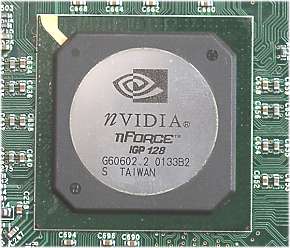 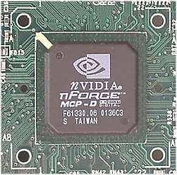 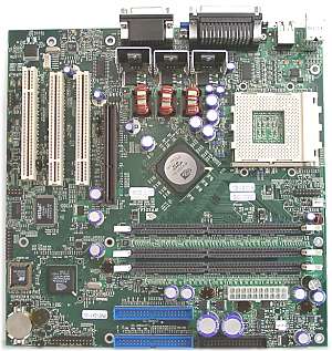 The board is of the mATX format. The layout, however, has a long way to go: all elements are too close to each other. As the board represents the chipset the developers did their best to realize all possible functions, hence the heaps of connectors. But I can't give you a detailed description as we received only a "bare" board. The nForce chipset supports SDR SDRAM but the sample we got has no connectors for this memory type.  We installed Corsair PC2400 modules of 2400 GBytes/s bandwidth. The memory works as 133 MHz; and the benefit can be obtained only by decreasing delays of the PC2400 whose rated frequency is 150 MHz. 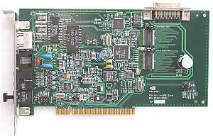 The board has two PCI slots and one ACR. Besides, there is an extension card for the latter slot which has most of the necessary connectors: a network controller, a modem or HomePNA, an optical output (Toslink) and outputs for a central channel, a subwoofer and rear speakers. Here are the connectors of this card:   The connector on the right will be removed in production boards The chipset incorporates a graphics core, that is why the typical place of the second serial port is taken by a VGA connector, and the port is made in the form of a connector which can be coupled with a bracket for the front or rear computer panel. The north bridge is left without a heatsink, for some reason. I/O ports are protected by fuses. 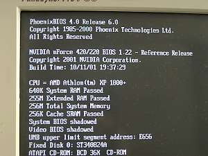 The BIOS is based on the Phoenix prototype and lacks for many interesting functions, for example, you can't change a FSB frequency (except 66, 100 and 133MHz), though you can set a correlation of PCI, AGP and FSB frequencies. Among settings for memory timings there is only a choice of CAS latency and some vague "Normal mode" and "nForce Turbo Mode" (we used the latter all the time). Of course, you can turn on/off PCI devices such as a sound controller. A size of a frame buffer can be up to 32 MBytes. After installation of the drivers the Device Manager gave out the following information: 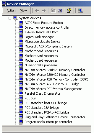 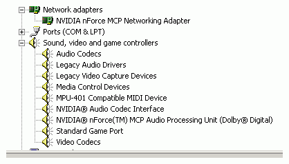 Mind two Memory Controllers; their joint operation provides 128-bit memory access (one of two modules has to be inserted into the DIMM1 connector). Examination of the memory subsystem is the first stage of our tests. The integrated GeForce2 MX core is identified as a usual GeForce2 Integrated GPU video card with 32 MBytes memory: 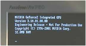 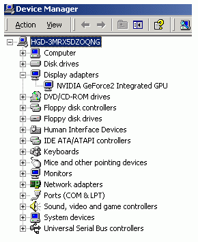 These 32 MBytes are included into the total memory size. The standard driver from NVIDIA has an overclocking tab but frequencies of the chip (175MHz) and memory (133 (266) MHz) can't be changed. 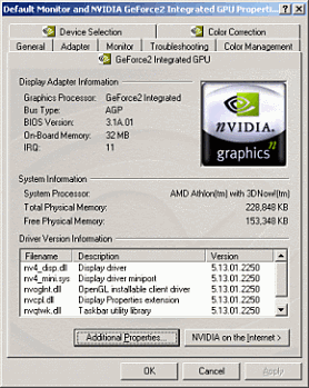 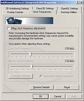 The performance of the integrated graphics chip must go on a par with the GeForce2 MX, and an in-depth comparison of these two video solutions is the second stage of our tests. The Leadtek WinFast GeForce2 MX MAX (MX 400) will participate as a competitor. Its chip operates at 200 MHz, and its memory works at 166 MHz (it is 64 MBytes SDR SDRAM). In closing I should note that the board was highly stable in operation. Competitor: VIA KT266A based boardThe competitor for the nForce is the Epox 8KHA+ board. The VIA KT266A chipset turned out to be a winner in the recent comparison of chipsets for AMD processors, and the Epox represented this chipset in our lab. The nForce vs. KT266A is the third stage of our tests. Epox 8KHA+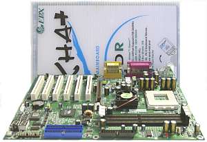 The company has just added "+" to the board's name demonstrating a higher performance of the new chipset from VIA. It differs from its predecessor 8KHA only in the chipset and in a higher-quality AC'97 codec from Avance Logic. The today's board packed in a semitransparent plastic box is supplied with 40- and 80-conductor cables for IDE devices, an FDD cable and a bracket with two additional USB connectors or the rear computer panel. A thick board description gives you all necessary instructions for installation of the board and drivers. A folding short manual is written in 6 languages. Besides, there is a CD with drivers and a modest set of freeware programs, among which are Adobe Acrobat Reader 4.05, Norton Antivirus 2001, PCCillin 2000 and Norton Ghost 6.03. Besides, there is a utility for measuring a processor frequency from DOS or Windows - Boostek. 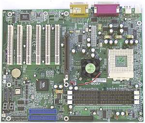 CD-in and AUX-in connectors are placed in front of the first PCI slots - it has nearly become a standard for the manufacturers, but it isn't convenient for assemblers. Besides, the company has decided to save on plastic for these connectors. The cables will undoubtedly fall out from such connectors. On the other hand, there is a clamp on the AGP connector and an AAVID's cooler on the north bridge of the chipset. Besides, there are two standard 7-segment LEDs for monitoring the POST procedure. The codes displayed on them are described in the manual. The feed circuits have 12 LowESR capacitors of 2200uF each. 2 switches are meant for clearing the CMOS and for choosing the base frequency - 100 or 133 MHz. All other settings can be made from the BIOS Setup. The BIOS is based on the v6.00 from Award and includes a great deal of possibilities for adjusting memory timings, AGP and PCI buses operation and a possibility to distribute manually interrupts among PCI slots. The FSB frequency can be changed from 100 to 200 MHz in 1 MHz steps. The core voltage can be changed +/- 0.1V in 0.025V steps and the memory voltage can be lifted by 0.7V from the rated value in 0.1V increments. And now take a gander at the characteristics of the two boards in question:
PerformanceTest system:
Software:
Let's start with the synthetic test WStream. 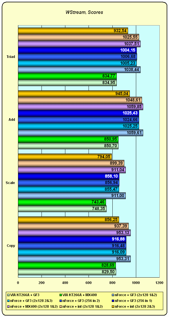 This test works aggressively with large vectors measuring a peak performance of the memory subsystem. The results are the following:
I should add that we have conduncted tests of the memory subsystem with the Cachemem but the results turned out to be too queer and I had no desire to display them. Such a strange operation of the nForce in some synthetic tests is caused by the DASP. If a memory access is chaotic or too complicated for prediction with the DASP algorithms, the pre-fetch can decrease the productivity. Unfortunately, we couldn't disable the DASP to carry out the comparison. Now comes the group of applications which are a burden, first of all, for a processor. 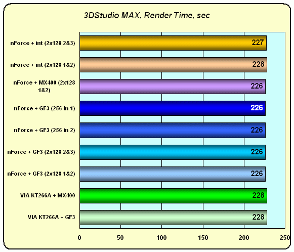 Absolutely equal results. 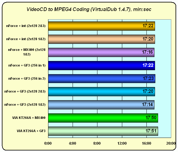 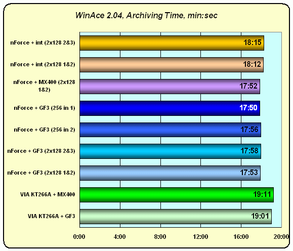 We do notice the difference, but in these applications, which are tough for the processor and have chaotic algorithms, the DASP provides for the nForce a lead of 23% over the KT266A. In the WinAce all test platforms which use integrated video lag behind by a little margin because of the user interface. 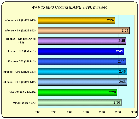 The results are quite strange, though we conducted the tests several times. 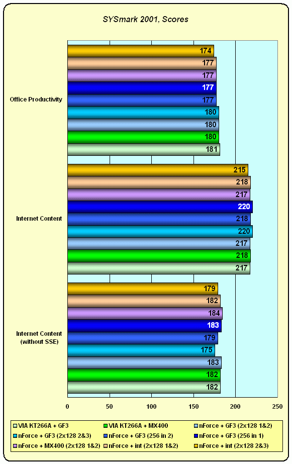 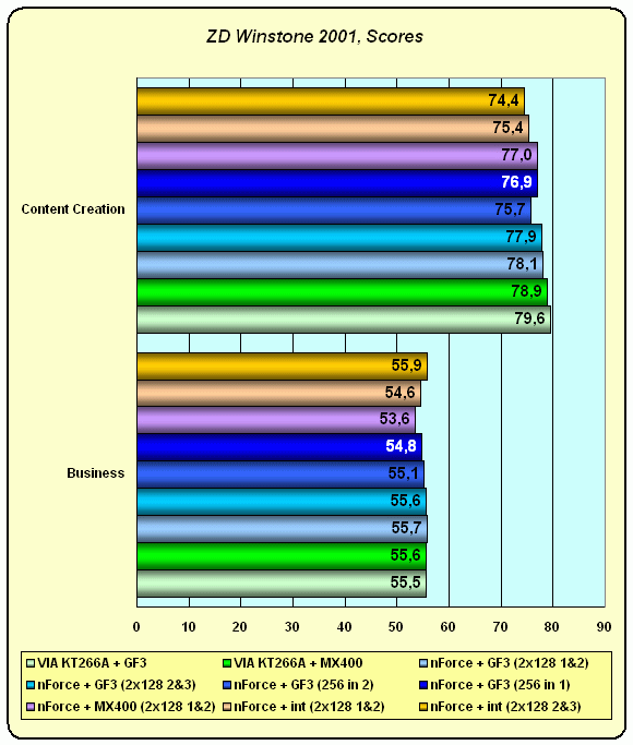 The business class applications: the SysMark and ZD Winstone results are the same given the possible inaccuracy of measurements. 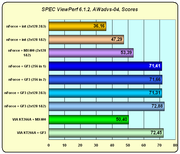 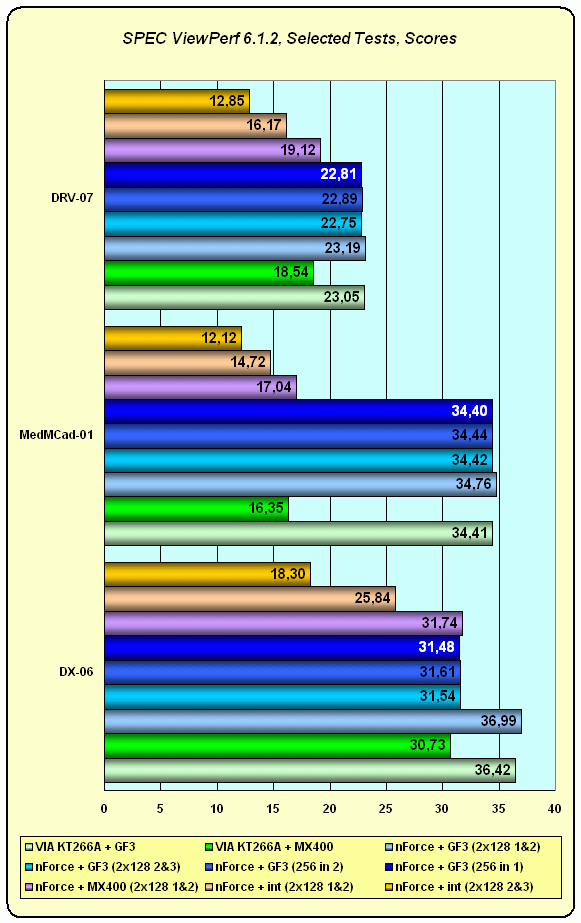 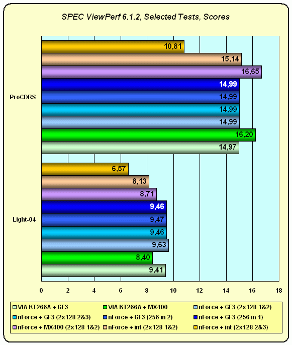 The systems based on the GeForce3 are leading regardless of the chipset and a memory speed - the systems are limited by the bond of a processor and video drivers, and, possibly, an AGP bus. The external GeForce2 MX beats the internal one everywhere - these tests require a rapid operation with memory; here the integrated accelerator competes against a processor for the memory access. Besides, the external one had a speedier chip and a more efficient T&L. The nForce, at the same time, has a higher score than the KT266A. The difference between 64- and 128-bit access is well seen on the integrated video chip which gasps when the bus is cut to 64 bit. The only outstanding result is in the DX-06 test. Here, a memory bandwidth matters most of all, and the external GeForce2 MX with 128-bit access outscores all GeForce3 processors with a 64-bit one. The results prove that the ViewPerf tests carried out on the modern accelerators depend mainly on the platform (processor+chipset+memory). 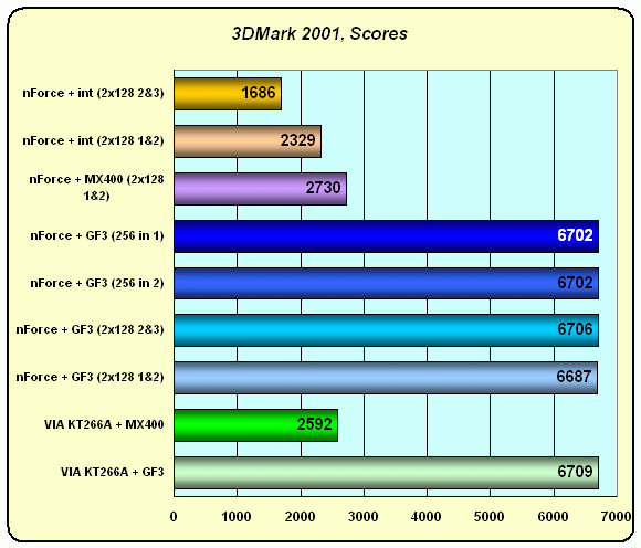 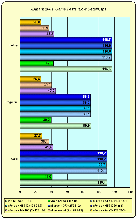 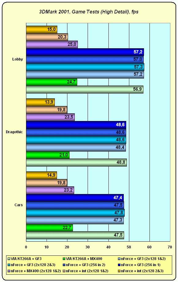 The similar situation takes place in all 3DMark tests. With the GeForce3 the performance is limited by the accelerator, the external GeForce2 MX works much faster on the nForce due to a quicker memory access, while the integrated video yields to it (especially with a 64-bit bus). Finally, we have games. 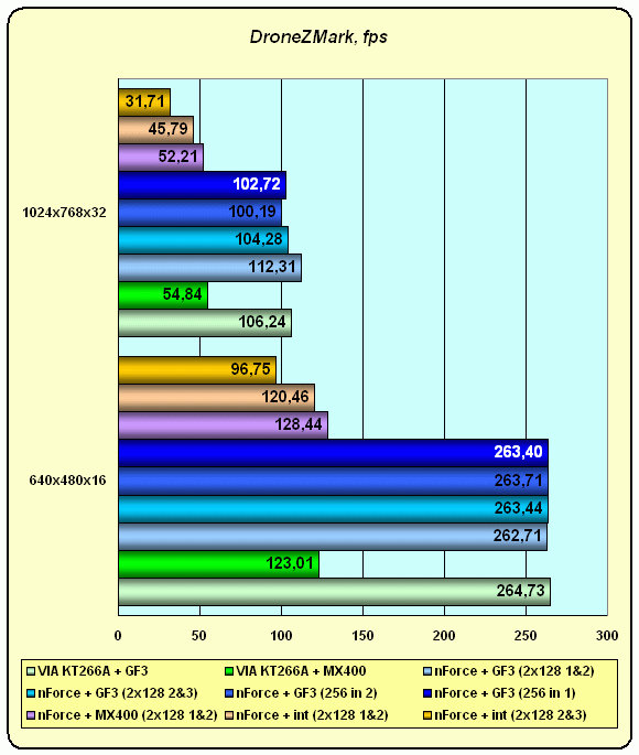 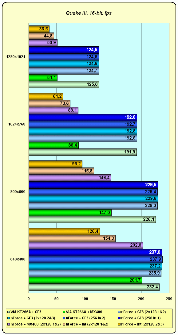 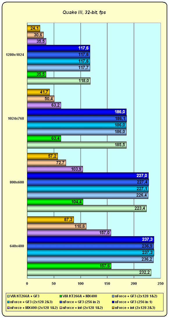 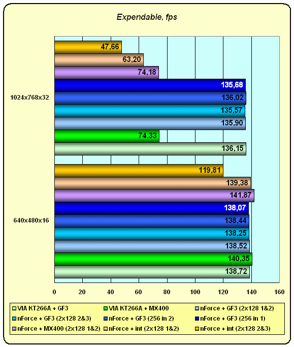 It is the same OpenGL and we get the same results (except the 640x480 mode in the Expendable - the overall performance is limited by the platform because of too simple graphics). Another aspect to be pointed out is a weighty DroneZmark - with the maximum settings the 128bit bus loads the GeForce3 much more and lifts the total fps. SummarySo, we have a new performance leader among chipsets for Athlons. The nForce snatched out the palm from the today's best chipset. The speed of operation with memory is really impressing, especially if a test "suits" for DASP. Real applications don't get a considerable gain, and the NVIDIA even loses to the VIA with a 64-bit bus. But first of all, I think it makes no sense to use a 64-bit mode, secondly, performance of most applications (in particular, games) can benefit much from a 128-bit access, and thirdly, we tested just a reference board... In all tests the external accelerator outclasses the integrated one even in case of the 128-bit memory access. But we should take into account that the external GeForce2 MX has better characteristics. I think the price will be a determining factor here. The chipset is the most efficient in its group and has a promising potential. But remember that you have to get two DIMMs and a powerful accelerator to play modern games. However, apart from the above results and price
of the nForce you should take into account its communicational and
sound possibilities which will be considered in the near future.
Write a comment below. No registration needed!
|
Platform · Video · Multimedia · Mobile · Other || About us & Privacy policy · Twitter · Facebook Copyright © Byrds Research & Publishing, Ltd., 1997–2011. All rights reserved. | ||||||||||||||||||||||||||||||||||||||||||||||||||||||||||||||||||||||||||