 |
||
|
||
| ||
|
||
|
||
| ||
ArchitectureThe first generation of unified GPUs from NVIDIA (GeForce 8 and 9) were based on the scalable array of processors. The second generation of the unified architecture to be reviewed today has a similar but improved basis. The array contains a certain number of TPC units (Texture Processing Clusters), each of which includes several streaming multiprocessors (SM). Each SM, in its turn, consists of several streaming processors (SP) -- that's what marketing reviews count and compare. Streaming multiprocessors also contain texture fetch and filter units, which are used both in graphics and some computing tasks. The new generation of NVIDIA GPUs improved its computing performance relative to previous G80 and G92. Firstly, the number of streaming multiprocessors (SM) per each TPC unit has been increased to three versus two units in the previous generation. Secondly, the number of TPCs in the GPU has been increased from 8 to 10. As a result, we get 10 * 3 * 8 = 240 streaming processors in one GPU. Here is the basic diagram of GT200: 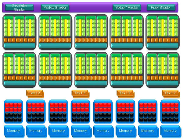 Everything is just like in G80, only the diagram got brighter. You can see a dispatcher in the upper part of the diagram -- this control logic manages execution of multiple shaders. You can also see triangle setup and other units there. Then we have ten TPC units, each of which includes 24 streaming processors and 8 texture fetch and filter units. ROP units, linked to the memory exchange interface, are in the lower part of the diagram. Here is a detailed diagram of the TCP unit: 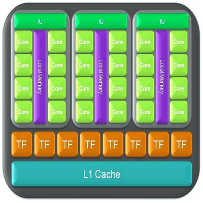 Nothing new, we notice only quantitative changes and added FP64. By the way, each TCP contains local memory (16 KB) shared between all streaming processors in a unit. Here is a photo of GT200 with specified areas of corresponding execution units, so that you could see how much of the GPU surface is taken by various units. 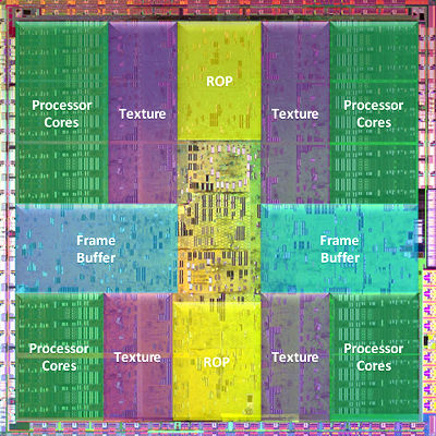 Control logic is probably placed in the center. Caches are not large (compared to CPUs), and they are not displayed on the diagram. But they exist. As you can see, streaming processors take up most of the surface. But TMU and ROP units are also large, the former units occupy almost as much surface as shader processors. The increased number of transistors and larger GPU surface area are easy to explain -- compared to G80 and G92, GT200 has more units of every kind, no exceptions. All these quantitative and qualitative changes significantly raised efficiency of the new architecture relative to the previous generation. Now we are going to analyze each modification in the new generation of GPUs. Increased number of simultaneously executed threadsOne of the most important features of GT200 is its support for more than 30000 threads. Its control logic makes sure that all streaming processors are loaded by 100%, not idling away. Each SM can execute up to 1024 threads simultaneously. So thirty such units in GT200 can cope with 30720 threads simultaneously. Compare this number with 768 threads per SM and 12288 threads per GPU in previous solutions based on G80 and G92. This change should raise performance and flexibility of both parallel and complex graphics computations. Unfortunately, NVIDIA does not publish statistics, so it's difficult to judge real performance gains. Increased size of the register fileThe size of the local register file in each SM of the new GPU has been doubled relative to G80 and G92 Previous solutions sometimes came up against situations, when performance of long complex shaders was limited by insufficient space for registers, and their values were moved to memory, which slowed them down. The increased register file size in GT200 allows to execute long complex shaders faster and with higher efficiency. This solution certainly raised complexity of the GPU and made it bigger, but the register file takes up only an insignificant part of SM area. In return, increased complexity of shaders in games and applications will result in performance gains, when many registers are required. According to NVIDIA's data, a twice as large register file yields a 10-15% performance gain in 3DMark Vantage. It's a very good result for such an extensive modification in a GPU. Dual IssueDual Issue is a technology to execute two instructions per cycle in one shader (in this case it's MAD+MUL). Each SM contains special function units (SFU). They compute complex functions, interpolate attributes, and do multiplication (MUL). Each streaming processor in GT200 can use them to execute not only one multiplication with addition (multiply-add -- MAD), but also MUL at the same time. MAD operations are executed by streaming processors, while SFU does another multiplication operation. Optimized tests use this feature with nearly 100% efficiency. This very feature helps the new NVIDIA cards reach peak theoretical performance of almost one gigaflop for single-precision floating-point computations. Support for double-precision computationsSingle-precision is not the only feature the new GPU can boast of. GT200 has a very important addition for computations (CUDA, etc) -- support for floating-point computing of double precision (64-bit). It's necessary for a number of scientific, engineering, and financial applications that require high computing precision. For this purpose each SM contains a unit for mathematical operations of double precision, so this GPU contains 30 such units in total. Each of these units executes MAD with higher precision in compliance with IEEE 754R. Overall double-precision computing performance of all ten TPC units in GeForce GTX 200 reaches 90 gigaflops (peak performance), which is similar to the power of an eight-core Xeon CPU. Higher texturing performanceThe old top GPU from NVIDIA (G80) contained eight TPC units, each having eight texture filtering units (64 pixels per cycle) and four texture address units (32 pixels per cycle). They can fetch 32 8-bit pixels per cycle, including anisotropic filtering 2x, or just as many bilinear filtered 8-bit or 16-bit values. G92 tipped the balance to more address units, this GPU can fetch and bilinear filter 64 pixels per cycle for textures with 8 bit per channel and 32 pixels with 16-bit floating-point values. The new GPU also contains the same number of texture address and filtering units per TPC. Each of them includes eight texture units that can fetch and filter eight pixels per cycle, or four pixels with anisotropic filtering, or four pixels in FP16 format. So GT200 can do 80 or 40 pixels per cycle correspondingly. Thus, texturing efficiency has grown since G92 only owing to the increased number of corresponding units. But NVIDIA tells us that GT200 features more efficient control logic, which allows to achieve practical texel rates closer to the theoretical maximum than the previous GPUs (we speak of G92, which had some problems here, we mentioned them in our reviews). According to their own measurements, texturing efficiency of the new GPU is higher by 22% (compared to G92). We are going to test it in the next part of the review. Modified ratio between numbers of various execution unitsIt's just a consequence of architectural modifications. The number of texture units hasn't grown as much as the number of computing units. So their ratio has changed. This has become useful, because games and other applications use increasingly complex and long shaders, so performance is limited by computing, not by texture lookups. That's why they shifted the balance in GeForce GTX 200 to a higher SP-to-TMU ratio. Engineers added one SM to each TPC, preserving the number of texture address and filter units, so this ratio has grown by 1.5 compared to G92. This decision was made after a performance analysis of modern and future games and applications (NVIDIA works with game developers). ROP improvementsThe previous generation of G80 GPUs used improved ROPs, and GT200 also has its ROPs overhauled. All basic features are preserved, but performance of these units is increased owing to the extensive growth. They can now output up to 32 pixels per cycle, 4 pixels per each wide ROP unit (eight in total). The same concerns color and Z values -- up to 32 pixels. Pixels in the 8-bit format can be output with blending at the double frequency relative to the previous generation of GPUs. Old GPUs have six wide ROPs and can output 24 pixels per cycle and blend 12 pixels. GT200 can output 32 pixels per cycle with blending in these conditions. Modified geometry shader and stream out unitsPrevious generations of unified GPUs from NVIDIA demonstrated weak geometry/stream out performance in some cases. In particular, it could be seen in one of geometry shader tests in the second version of our synthetic RightMark benchmark. Internal buffers of GT200 were significantly enlarged to solve the problem -- they are several times as large as the ones in G80 and G92. It helps the new GPU demonstrate significant performance gains in such tasks that actively use geometry shaders and stream out. According to NVIDIA, GeForce GTX 280 demonstrates much higher results in our RightMark 3D 2.0 than GeForce 9800 GTX, and it outperforms some of competing products. We'll check it up as well. Other architectural improvementsJudging by the company's data, there are other improvements in this GPU to increase performance and efficiency of the new architecture. They optimized the memory interface between a data assembler and frame buffer units, so GT200 gets faster access to indexed primitives. The previous generation experienced some problems in these conditions. Caches were enlarged to reduce idle time of the pipeline and accelerate communications between its geometry and vertex stages with viewport clip and cull. Z-Culling performance is also increased, which should be especially noticeable in high render resolutions. We've already written about ROP improvements above. Some modifications and improvements were introduced into the microarchitecture, which have to do with registers, control logic for threads and instructions. GT200 feeds data to various execution units more efficiently than older GPUs. These changes also allow shader units execute two operations per cycle simultaneously, we've mentioned this feature above. 1 GB of video memoryStrictly speaking, it's not a GPU improvement, older solutions could also be equipped with 1 GB of memory or even more. But nevertheless, modern games require much video memory. They use more geometry, textures with normal maps of higher resolutions, shadow and environment maps in 16-bit formats, and several high-res buffers (for post processing and deferred rendering, for example). Many modern technologies have high requirements to video memory size and bandwidth. To say nothing of multisampling, which also has a strong effect on these requirements. GeForce GTX 280 cards support video memory size of 1 GB, which allows to raise performance in cases of insufficient video memory, in high resolutions with enabled antialiasing. 512-bit video memory busThat's an apparent improvement versus G80 and G92. GT200 uses 512-bit access to local memory, unlike 384-bit access in G80 and 256-bit access in G92. As in previous GPUs, it uses 64-bit memory exchange units, but now there are eight of them instead of four or six. So the bus width and memory bandwidth have grown accordingly. Video memory usage efficiency has been improved as well. Frame buffer units were overhauled for higher memory frequency, algorithms of caching data and access to memory banks were modified. Data compression technologies of GT200 were improved to raise its results in heavy modes. No support for DirectX 10.1GT200 does not support all features of DirectX 10.1, even though many users were expecting it. NVIDIA explains the lack of this support in the following way -- this API version includes a non-critical DirectX 10 addition, some of its features are available to GeForce cards of the eights series and higher, for example, reading data from a multisampling buffer. According to the company, software developers admitted that DirectX 10.1 support is not critical for them, so the company decided not to modify its GPUs and concentrate on raising performance of existing functions and efficiency of existing units. This approach is not acceptable in some cases, but it explains NVIDIA's decision. Write a comment below. No registration needed!
|
Platform · Video · Multimedia · Mobile · Other || About us & Privacy policy · Twitter · Facebook Copyright © Byrds Research & Publishing, Ltd., 1997–2011. All rights reserved. |


