Architecture
Let's proceed to the boring part. We have nothing to add to what we have already published. RV770 hasn't been modified. Its architecture has been described in detail in the corresponding article. Let's dwell on some peculiarities of using multiple GPUs. In the times of HD 3870 X2 we mentioned that it did not support PCI Express 2.0, even though it was one of the key innovations in the RV670. That graphics card used a special PCI Express bridge (PLX PEX 8547) to connect its two GPUs, which supported 48 lanes of PCI-E 1.1. Back then AMD had planned to integrate this PCI Express bridge into future GPUs.
Let's see what has been done in HD 4870 X2. The dispatcher is still installed between two GPUs to link them. To all appearances, this chip belongs to the so-called "second generation of PCI Express bridges" manufactured by the same PLX Technology, one of the leading manufacturers of PCI Express solutions for input/output systems and internal wiring. As the company has no products with a similar designation (see the photo further), this chip might have been manufactured specially for AMD. Its characteristics resemble those of PEX8647, which is proved by documentation published on the official web site.
The second generation of PLX bridges was announced in the beginning of 2008. It's notable for relatively low latencies (140 ms), very low power consumption (about 3.8 W), and flexible configuration. This bridge provides three PCI-E ports compliant with Specs 2.0, 16 lanes each. Sixteen PCI-E lanes are dedicated to connect to each RV770, and just as many lanes are used to exchange data between a motherboard and a graphics card. The new model differs from PEX8547 (used in HD 3870 X2) in PCI Express 2.0 support, smaller package dimensions, and better power saving (the old solution consumed about 5 W).
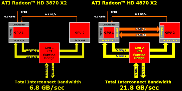
Let's analyze the diagram of links between the GPUs and a motherboard, provided by AMD. It compares HD 3870 X2 and HD 4870 X2:
You'll notice right away theoretical values of general bandwidth, which differ three-fold in these generations: 21.8 GB/s versus 6.8 GB/s (that's the total in all directions, of course). Well, let's find out where this difference comes from. Firstly, it's the effect of the bridge supporting PCI Express 2.0 instead of 1.1. This feature provided a greater part of bandwidth, doubling it in all directions. External link with the bandwidth of 0.9 GB/s hasn't changed. But the secret sideport, mentioned in early diagrams of RV770, turned out to be an additional port (similar to a 16-channel PCI-E 2.0, judging by its bandwidth) solely for data exchange between the GPUs, by-passing the bridge and a motherboard.
Will it provide any serious advantages? Unlikely. Just because the main part of limitations has to do not with bandwidth between GPUs, but with peculiarities of used algorithms. Well, theoretically, data exchange (off-screen render buffers) must go faster, but it's hardly the main limitation of AFR performance. It would have been interesting to compare performance of a single HD 4870 X2 and two HD 4870 cards (with 1 GB of video memory and operating at the same frequencies) in CrossFire, in order to evaluate contribution of this interchip channel. But in its documents, AMD prefers to compare the speed of the new card with 512 MB modifications of HD 4870 in CrossFire, obtaining performance advantages, as the latter cards suffer from insufficient video memory in heavy modes.
HD 4870 X2 itself operates as a dual-GPU system, but ATI CrossFireX technology allows to connect two such cards on a single motherboard. According to AMD, such a system provides high efficiency of multi-GPU rendering in high resolutions with antialiasing and anisotropic filtering, performance gains from each GPU reach 75-80%.
As you can see, this dual-GPU card offers excellent technical characteristics and theoretical opportunities. Taking into account the power of the single-GPU modification, HD 4870 X2 must perform brilliantly in synthetic and game tests. And now a little fly in the ointment. We wrote once that AMD mentioned problems of large High-End GPUs (they apparently meant GT200 from NVIDIA). These problems included too high costs and power consumption, long delays before new fabrication processes are adopted, because less complex GPUs are easier to upgrade to thinner processes. We can agree with the last statement (even though it's not a proved fact). But let's think about the first point.
So, AMD positions RADEON HD 4870 X2 and HD 4850 X2 as competitors to GeForce GTX 280. Let's compare prices and official power consumptions. For AMD cards it's 230/286 W and $399/549. What concerns GTX 280, it's 236 W and $499. Where are the promised advantages? Even if we don't pay attention to prices (we don't know manufacturing costs, but a dual-GPU card is hardly cheaper than a single-GPU card). Where is lower power consumption of HD 4850 X2 versus GTX 280? What will change when GT200 is switched to the 55-nm fabrication process? These are rhetorical questions...
That's the end of the first part, as we already know all theoretical details on RV770 and CrossFire. So we proceed to the next part of the article with tests. We'll evaluate performance of the new solution based on two RV770 chips in comparison with other cards from AMD and competing cards from NVIDIA.
Write a comment below. No registration needed!

