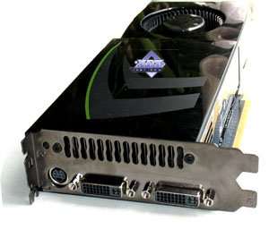
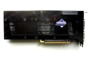
NVIDIA GeForce GTX 260 896MB
|
And again we return to California. NVIDIA continues to roll out new products with tenacity to be respected by other companies. The novelties differ only in the number of unified shader processors. There were cards with 32, 64, 96, 112, or 128 of them. Now we also have products with 192 and 240 shader processors. What's left: 192-24 = 168, 168-24 = 144, and 192+24 = 216. Each different by 20 bucks, such products will make the series complete and suitable for all occasions. Each solution should bear one of these suffixes: "+", "++", "Super+", "Great+", "GTXer", and "GTXest" along with marketing cliches about revolutional technologies. When this vocabulary is finally depleted, they can stop and think about inventing something new.
Anyway, today we are going to review a graphics card that has the same dimensions and weight as the GTX 280, but it has a narrower bus and fewer unified processors. Besides, it's noticeably cheaper. Meet the GeForce GTX 260.
Since GTX 280 is priced too high, while the GTX 260 doesn't exceed 400 USD, the latter will probably be more popular. Let's see what exactly it can offer for these money.
Graphics Card
| Reference NVIDIA GeForce GTX 260 896MB |
- GPU: GeForce GTX 260 (GT200)
- Interface: PCI-Express x16
- GPU frequencies (ROPs/Shaders): 575/1240 MHz (nominal - 575/1240 MHz)
- Memory frequencies (physical (effective)): 1000 (2000) MHz (nominal - 1000 (2000) MHz)
- Memory bus width: 448bit
- Vertex processors: -
- Pixel processors: -
- Unified processors: 192
- Texture processors: 64 (BLF/TLF)
- ROPs: 24
- Dimensions: 270x100x33 mm (the last figure is maximum thickness of the graphics card).
- PCB color: black
- RAMDACs/TDMS: in a separate NVIO chip.
- Output connectors: 2xDVI (Dual-Link/HDMI), TV-out.
- VIVO: not available
- TV-out: integrated into GPU.
- Multi-GPU operation: SLI (Hardware).
|

|
| Reference NVIDIA GeForce GTX 260 896MB |
| The graphics card has 896 MB of GDDR3 SDRAM allocated in 14 chips (seven chips on each side of the PCB.) Hynix memory chips (GDDR3). These memory chips are designed for the maximum frequency of 1200 (2400) MHz. |
 |
| Comparison with the reference design, front view |
| Reference NVIDIA GeForce GTX 260 896MB |
Reference NVIDIA GeForce GTX 280 1024MB |

|

|

|
| Comparison with the reference design, back view |
| Reference NVIDIA GeForce GTX 260 896MB |
Reference NVIDIA GeForce GTX 280 1024MB |

|

|

|
As we can see, this card is a copy of the GTX 280, but it lacks two memory chips. As a result, the memory bus has shrunk from 512 to 448 bit, and memory size has been decreased from 1024 MB to 896 MB. Besides, the 8-pin power connector is replaced with a usual 6-pin connector (two of them). However, the PCB bears a 512-bit memory exchange bus. Engineers had to arrange 16 memory chips (only 14 chips are installed), which required the double-sided arrangement of the chips (eight chips on each side). So the card is long, and the PCB is quite expensive. Don't forget that NVIDIA again brought all data output units into a separate NVIO chip like in the G80 (8800 GTX/Ultra).
Write a comment below. No registration needed!
|
|
 |
|
|
|
