 |
||
|
||
| ||
|
||
|
||
| ||
Cypress architectureThe overhauled architecture of the new Cypress GPU is called TeraScale 2. Figure 2 stands for the generation and points indirectly to the number of full theoretical teraflops (billion operations per second) that the GPU can don. So, the new GPU is notable for doubled performance in key theoretic parameters compared to the previous generation. Its peak arithmetic performance exceeds two teraflops, just a little short of three teraflops actually. As usual, when engineers designed the new GPU, their main objective was to increase its efficiency. They had to achieve a two-fold advantage in theoretical performance over the prev-gen GPU. With the GPU complexity of 2.15 billion transistors (over twice as many as in the top GPU of the previous generation), Cypress is bigger than RV790 by one third -- 334mm2. It's quite acceptable for the 40nm process technology. One can say that the new GPU has no cardinal changes, it's just a development of the previous generation. However, minor modifications have been introduced almost to all its units: stream processors, texture units, ROPs, output controllers. These are minor modifications, so the GPU scheme hasn't changed much: 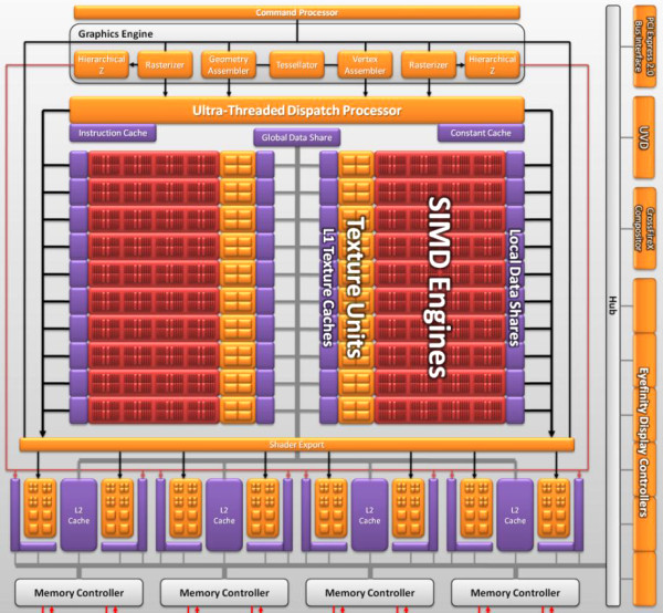 We can see that Cypress architecture resembles the RV770 very much, and it's hard to find anything new here. But there are still some changes here. Let's examine them in detail. One of the important changes is the addition of two raster units. This modification will not affect performance in old tasks, which are not limited by raster speed, but it will be very useful for new features of DirectX 11, especially tessellation. 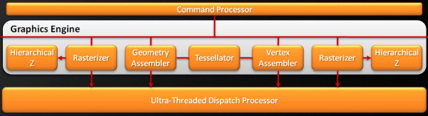 As we know, tessellation has been supported by AMD GPUs for a long time. But DirectX 11 has different requirements to hardware, so the tessellator was improved in Cypress. According to AMD, it's already the sixth generation of hardware tessellation. We leave it up to our readers to count all previous generations. As for us, we haven't counted five generations, if we don't take into account the long forgotten TRUFORM. The main part of the Cypress chip consists of twenty SIMD cores (twice as many as in the RV770), each one containing 16 blocks of superscalar streaming processors, 320 all in all. The superscalar nature of these processors hasn't changed since RV670. So we can say that the GPU contains 320*5=1600 scalar 32-bit streaming processors. The same units are used for 64-bit computations of double precision, but the computing rate drops. 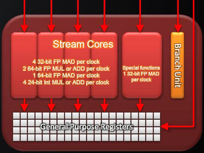 Each stream processor contains four execution units and one special unit, as well as a branch unit and general purpose registers. Everything is just like in the RV770. A lot of stream processors provide high performance on a level of 2.7 teraflops in single-precision computations. Superscalar stream processors allow AMD to implement effective support for double precision computing (FP64) using the same units. As a result, Cypress offers peak performance in FP64 computations of up to 544 gigaflops. It's significantly higher than in previous products, especially in competing cards. AMD has increased the number of instructions executed per cycle (IPC), units can execute co-issue MUL and ADD instructions per cycle. There also appeared a new command -- Sum of Absolute Differences (SAD). All these improvements should raise efficiency of generic and graphics computing. As you may remember, the RV770 had significantly modified texturing units, and each SIMD contained four texturing units. The same ratio has been preserved in Cypress -- 80 TMUs all in all. Peak texturing performance has been raised owing to the increased number of units. This GPU can fetch up to 272 billion non-filtered 32-bit samples per second, which corresponds to 68 billion bilinear-filtered texels per second. But TMUs still needed some minor improvements. DirectX 11 has brought the requirement to support addressing textures of up to 16384x16384 as well as new compression algorithms for 32-bit and 64-bit HDR buffers (BC6/BC7). Besides, texture units can now read data from compressed MSAA buffers. Quantitative changes and DX11 requirements are not the only features the new GPU can boast of. It uses a new algorithm of anisotropic filtering, which offers improved quality, when mip levels are arranged in perfect circles. AMD mentions that it happens without deteriorating performance. However, quality and performance of anisotropic filtering in the new GPU is a question for a separate article. As for now, we'll publish a picture provided by the manufacturer: 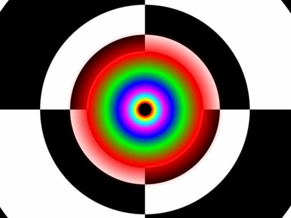 All texturing improvements would have made little sense without proper support by the caching system. According to AMD, L1 cache bandwidth has grown to 1 TB per second (480GB/s in the RV770), and the throughput between L1 and L2 has become 435GB/s (versus 384GB/s in previous chips). The caching system remains the same: L2 cache is tied to four 64-bit memory channels, L1 caches store unique data for each SIMD to raise caching efficiency. L2 cache size has been doubled proportionally to the increased number of TMUs -- it's reached 128KB per memory controller. ROPs (Render Back-Ends -- RBE) remain practically the same as in the RV770. They process the same number of pixels per cycle, there are just twice as many ROPs now, that's all. Blending performance has also been doubled (compared to the RV770). This GPU processes 32 pixels per cycle in 2x/4x MSAA mode, 16 pixels -- in 8x MSAA. These values hold true both for 32-bit and 64-bit buffers. MSAA 2x and 4x algorithms come practically free of charge for ROPs (we still have questions about memory bandwidth and buffer compression efficiency with MSAA, for example). In practice, rendering speed in 8x MSAA mode is lower than in 4x MSAA mode only by 10-15% (according to the manufacturer). It's a very good result, especially if you like high graphics quality. Cypress features higher performance of CFAA, MRT, and color buffer. AMD does not provide more information, so we'll have to test the cards to get more data. Along with CFAA, the new chip now supports SuperAA to antialias not only polygon edges, but also textures, and pixel shaders. It's not just a software solution, the company speaks of an efficient method using adaptive antialiasing. We'll leave it off for a special image quality review. GDDR5 memory controller has been optimized once again, so that it supports chips operating at up to 5GHz. What concerns improvements that don't have to do with performance, we can mention Fast GDDR5 Link Retraining, which allows to change memory voltage and frequency on the fly. There was added Error Detection Code (EDC) to the memory controller. It's irrelevant for graphics tasks, but CRC check can be useful for GPU computing tasks. Everything is just like in the RV770 in other respects. As you can see in the picture, there are no ring buses: 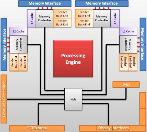 Let's mention a possible weakness of the new solution. It was of paramount importance to reduce production costs of the RV770, and GDDR5 bandwidth with a 256-bit bus was sufficient. But now memory bandwidth of Cypress barely exceeds 150GB/s with a 256-bit bus, which is only insignificantly higher than in the previous product. Unlike the other characteristics, it's higher only by one third than in RV770-based cards. And memory bandwidth may be one of the major bottlenecks of the GPU and graphics cards based on this product. Both in graphics tasks and in generic computations on the GPU. We'll check it up in the next parts of this article devoted to performance tests. And now we'll list all the other minor hardware modifications according to information provided by AMD. The new GPU offers improved performance of constant buffer refresh, faster geometry shaders, and modifications for professional applications: improved line rendering and 12-bit subpixel precision. The latter should help the card compete for the market of professional OpenGL graphics cards. Write a comment below. No registration needed!
|
Platform · Video · Multimedia · Mobile · Other || About us & Privacy policy · Twitter · Facebook Copyright © Byrds Research & Publishing, Ltd., 1997–2011. All rights reserved. |


