NVIDIA nForce 700a, GeForce 8000 Chipsets
|
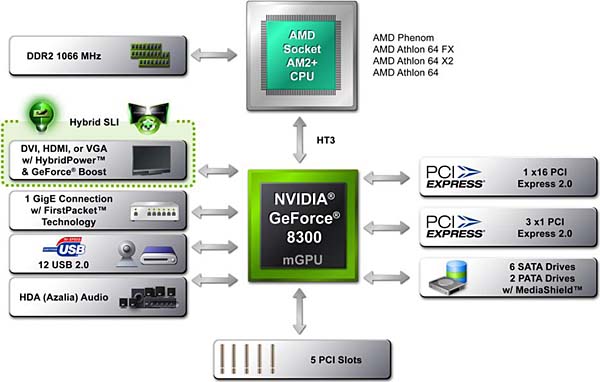
GeForce 8100/8200/8300
All three chipsets have the same functionality, they differ only in clock rates of the shaders in the integrated graphics core. The stock clock rate of the core in both cases equals 500 MHz, but frequency of the shader units in GeForce 8100 and 8200 amounts to 1200 MHz, in GeForce 8300 -- 1500 MHz. GeForce 8100 chipset does not support PureVideo HD, that is its HD video decode unit is locked. it always outputs the video signal to two receivers: via a digital channel (DVI or HDMI) and analog VGA.

The graphics core has 16 unified shader processors, four TMUs and four ROPs. Some of system memory is given to the core to use as video memory, it's impossible to install a dedicated video buffer on a motherboard. The number of PCI Express lanes is cut down to minimum (19 all in all versus 26 in AMD 780G), where 16 lanes are used for a graphics port, and other 3 lanes are used to install on-board controllers and expansion slots. All PCI Express lanes comply with the Specs 2.0. It must be noted that the available number of lanes must be sufficient for inexpensive motherboards, especially as the chipsets come with a built-in MAC adapter, so one lane is freed, which would have been otherwise occupied by a network controller.
Now what concerns the rest of functionality:
- Bidirectional HyperTransport 3.0 bus (up to 2.6 GHz, 16 bit in each direction) to a processor;
- 5 x PCI;
- Six Serial ATA ports for six SATA300 devices (SATA-II, the second generation of the standard), support for NCQ, TCQ, and Hot-plug;
- Two PATA133 devices (1 channel);
- SATA RAID 0, 1, 0+1, and 5
- MAC controller for 10/100/1000 Mbps network (Gigabit Ethernet) supporting traffic shaping and link redundancy;
- Up to twelve USB 2.0 devices;
- High Definition Audio (7.1).
nForce 720a/730a

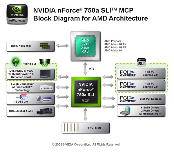
When you look at the diagram, it's rather hard to pinpoint the differences between nForce and GeForce models, now that graphics cores are integrated into chipsets. Have a closer look at the list of options. You will notice two differences: the lack of support for HDMI and support for just 16 PCI Express 2.0 lanes, while the other three comply with PCI Express 1.1 (in other words, only a graphics port gets double bandwidth). It must also be noted that all nForce chipsets are based on the graphics core similar to GeForce 8200, that is its shader processors operate at 1200 MHz. In other words, in this case the graphics core plays the second role, it's used in Hybrid Power. However, Hybrid SLI may still make sense for such boards, because these chipsets are addressed to the entry segment. Formally, they must be cheaper than similar motherboards on GeForce 8200. The 730a and the 720a differ just like GeForce 8200 and 8100 -- a cheaper modification has its video decoding unit locked. Perhaps, that's the way NVIDIA sells chips with a defected unit, or it may be a purely marketing decision. By the way, the list of chipsets includes a 710a model with the graphics core disabled completely. But we don't know about any motherboards manufactured or getting ready on this chipset.
nForce 750a SLI/780a SLI
nForce 750a copies the nForce 730a design with a single difference -- it may have two graphics ports, and 16 PCI Express lanes will be shared equally between two graphics cards. In fact, we have no problems with that. This configuration is quite acceptable for SLI based on inexpensive cards, considering double performance of PCI Express 2.0. The diagram also reveals the lack of the third PCI Express 1.1 lane. Well, we've already noted that NVIDIA decided not to spoil motherboard manufacturers with excessive chipset functionality this time.

Unlike other models, the flagship product in the series has a dual-bridge layout. However, all functionality of the South bridge is integrated into the Northbridge. And the second bridge is responsible only for graphics cards (three in this case). So graphics cards in 3-Way SLI mode form the x16+x8+x8 configuration. It stands to reason, as in case with a single card and the 750a chipset, it's possible to merge lanes, if you don't install the maximum number of cards. While previous SLI-chipsets from NVIDIA were criticized for their graphics slots' supported split between tow bridges. Theoretically, it might have affected the speed of cards' interaction. But in this case we have even a counterpart of Xpress Route (it's used in AMD chipsets to set up direct data exchange between the cards via the on-chip bus, PWSHORT). Besides, data can be sent from a CPU simultaneously to all graphics cards (Broadcast mode), for example, to send textures or geometry information to all cards at once. What concerns interaction between the NF200 bridge and the main chipset bridge, it's organized with PCI Express 2.0. Sixteen lanes (16 GB/s) must be enough for service data exchange with a CPU, as main traffic in SLI/CrossFire systems goes between graphics cards directly.
The nForce 780a chipset features two more "bonuses": support for SLI-Ready Memory (automatic configuration of memory modules for overclockers using additional data in EPP) and ESA certification (open standard that describes interaction between various PC devices in order to control multiple coolers and create optimal temperature conditions and minimal noise; however, this certificate means little in this case, first of all a user should buy an ESA-compatible PSU and PC case).
Write a comment below. No registration needed!
|
|
 |
|
|
|


