Qimonda DDR2-800 4GB Memory Modules
|
German Qimonda is one of the largest memory chip manufacturers. It offers probably the widest range of such products these days, including memory for mobile devices and the entire spectrum of RAM and video memory. Speaking of the latter, company's offer includes solutions up to GDDR5. And the official list includes 512 and 1024 Megabit chips. The order info is the standard "in production", and we all know where such chips are used these days.
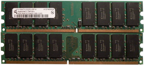
However, end users are interested not in memory chips, but in memory modules. It's much simpler to manufacture them from a technical point of view, but there are still certain issues. That's why memory modules made by chipmakers (e.g. Qimonda, Samsung, Hynix) are usually plain-looking reliable products that can operate at standard frequencies. While reviewers are less interested in such products, we have decided to examine an 8GB pair of Qimonda modules and find out how strong their performance might be affected by higher chip density and two-bank organization.
We shall not reason about who needs that much memory and why. Professional applications may require even more memory. But if we consider solely common users, who are not even interested in test results, only "look-and-feel", they will certainly notice how faster they are switching between applications (comparing to 4 GB memory). For example, it takes just a couple of seconds instead of dozens to switch from any modern game into a web browser. Great, isn't it? But it's up to you to decide whether the game is worth the candle: more expensive modules with lower overclocking potential vs. popular lower-capacity modules in a 64-bit operating system.
The manufacturer's website explains how to decipher Part Number of the modules. This document also lists most current production modules and their characteristics. However, we've found no information about our modules (the list mentions identical 4GB modules with ECC support, while ours do not support error correction).
Our 4GB modules are based on 16 BGA-package chips, 512M x 64. The manufacturer guarantees stable operation in DDR2-800 mode with 5-5-5 timings (RAS value is not mentioned in the description, SPD sets it to 18) at 1.8 V -- it's the default SPD mode. These memory modules come as OEM. So the manufacturer does not offer any selection or dual-channel kits.
SPD data
General description of the SPD standard: JEDEC Standard No. 21-C, 4.1.2 - SERIAL PRESENCE DETECT STANDARD, General Standard.
Description of the DDR2 SPD standard: JEDEC Standard No. 21-C, 4.1.2.10 - Appendix X: Specific SPDs for DDR2 SDRAM (Revision 1.2).
| Parameter |
Byte |
Value |
Interpretation |
| Fundamental Memory Type |
2 |
08h |
DDR2 SDRAM |
| Number of Row Addresses on this assembly |
3 |
0Fh |
15 (RA0-RA14) |
| Number of Column Addresses on this assembly |
4 |
0Ah |
10 (CA0-CA9) |
| Number of DIMM Banks |
5 |
61h |
2 physical banks |
| Data Width of this assembly |
6 |
40h |
64 bit |
| Voltage Interface Level of this assembly |
8 |
05h |
SSTL 1.8V |
| SDRAM Cycle time (tCK) at maximum supported CAS# latency (CL X) |
9 |
25h |
2.50 ns (400 MHz) |
| DIMM configuration type |
11 |
00h |
Non-ECC |
| Refresh Rate/Type |
12 |
82h |
They apparently meant 82h, which corresponds to 7.8125 ms -- 0.5x reduced self-refresh |
| Primary SDRAM Width (organization type) of the memory module chips |
13 |
08h |
x8 |
| Error Checking SDRAM Width (organization type) of the memory chips in the ECC module |
14 |
00h |
Not defined |
| Burst Lengths Supported (BL) |
16 |
0Ch |
BL = 4, 8 |
| Number of Banks on SDRAM Device |
17 |
08h |
8 |
| CAS Latency (CL) |
18 |
70h |
CL = 6, 5, 4 |
| Minimum clock cycle (tCK) at reduced CAS# latency (CL X-1) |
23 |
25h |
2.50 ns (400 MHz) |
| Minimum clock cycle (tCK) at reduced CAS# latency (CL X-2) |
25 |
3Dh |
3.75 ns (266.7 MHz) |
| Minimum Row Precharge Time (tRP) |
27 |
32h |
12.5 ns
5, CL = 6
5, CL = 5
3.33, CL = 4 |
| Minimum Row Active to Row Active delay (tRRD) |
28 |
1Eh |
7.5 ns
3, CL = 6
3, CL = 5
2 CL = 4 |
| Minimum RAS to CAS delay (tRCD) |
29 |
32h |
12.5 ns
5, CL = 6
5, CL = 5
3.33, CL = 4 |
| Minimum Active to Precharge Time (tRAS) |
30 |
2Dh |
45.0 ns
18, CL = 6
18, CL = 5
12, CL = 4 |
| Module Bank Density |
31 |
02h |
2048 MB |
| Write recovery time (tWR) |
36 |
3Ch |
15.0 ns
6, CL = 6
6, CL = 5
4, CL = 4 |
| Internal WRITE to READ command delay (tWTR) |
37 |
1Eh |
7.5 ns
3, CL = 6
3, CL = 5
2, CL = 4 |
| Internal READ to PRECHARGE command delay (tRTP) |
38 |
1Eh |
7.5 ns
3, CL = 6
3, CL = 5
2, CL = 4 |
| SDRAM Device Minimum Active to Active/Auto Refresh Time (tRC) |
41, 40 |
39h, 30h |
57.5 ns
23, CL = 6
23, CL = 5
15.3, CL = 4 |
| SDRAM Device Minimum Auto-Refresh to Active/Auto-Refresh Command Period (tRFC) |
42, 40 |
C3h, 30h |
195.0 ns
78, CL = 6
78, CL = 5
20.8, CL = 4 |
| Maximum device cycle time (tCKmax) |
43 |
80h |
8.0 ns |
| SPD Revision |
62 |
12h |
Revision 1.2 |
| Manufacturer's JEDEC ID Code |
64-71 |
7Fh, 00h |
Qimonda |
| Module Part Number |
73-90 |
-- |
64T512020EU25FA |
| Module Manufacturing Date |
93-94 |
07h, 48h |
Year 2007, Week 48 |
| Module Serial Number |
95-98 |
1Ah, 02h,
9Ch, 14h |
1A029C14h |
Three CAS# latencies are supported by SPD -- 6, 5, and 4. The first and the second values (CL X = 6 and 5) correspond to DDR2-800 (2.5 ns cycle time, 400 MHz) with the other timings being identical -- 5-5-18 timings (exact values). The third CAS latency value (CL X-1 = 4) corresponds to DDR2-533 (3.75 ns cycle time, 266.7 MHz) with nonstandard timings 4-3.33-3.33-12, which will be interpreted by most BIOS versions as 4-4-4-12.
SPD revision and Manufacturer's ID code are specified correctly. Part Number corresponds to the label on the modules, and Serial Number differs from the one on the sticker.
These modules do not support EPP extensions of the SPD standard.
Write a comment below. No registration needed!
|
|
 |
|
|
|