|
||
|
||
| ||
|
||
|
||
| ||
First Tests of Dual-Channel DDR3 Memory and Some Peculiarities of the Memory Controller in the Intel 3 Series Chipsets |
||||||||||||||||||||||||||||||||||||||||||||||||||||||||||||||||||||||||||||||||||||||||||||||||||||||||||||||||||||||||||||||||||||||||||||||||||||||||||||||||||||||||||||||||||||||||||||||||||||||||||||||||||||||||||||||||||||||||||||||||||||||||||||||||||||||||||||||||||||||||||||||||||||||||||||||||||||||||||||||||||||||||||||||||||||||||||||||||||||||||||||
| Parameter | Byte(s) | Value | Interpretation |
| SPD bytes (the number of bytes used for SPD, total SPD bytes, CRC area) |
0 | 92h | Bytes used: 176 Bytes in total: 256 CRC: Bytes 0-116 |
| SPD Revision | 1 | 10h | Revision 1.0 |
| DRAM type | 2 | 0Bh | DDR3 SDRAM |
| Chip capacity and the number of logical banks | 4 | 02h | Capacity: 1 GBit Banks: 8 |
| SDRAM addressing: Number of Row and Column Addresses on this Assembly | 5 | 11h | Number of Columns: 10 Number of Rows: 13 |
| Module organization: Internal Data Width of this assembly, Number of Physical Banks | 7 | 01h | Width: 8 bit Number of Banks: 1 |
| Data Width of this assembly (including ECC) | 8 | 03h | SDRAM Width: 64 bit ECC extension: not available |
| Fine timebase (FTB) (dividend : divisor) |
9 | 51h | 5 ps (5:1) |
| Medium Timebase (MTB) (dividend : divisor) |
10, 11 | 01h, 08h | 0.125 ns (1:8) |
| Minimum SDRAM Cycle Time (tCKmin) | 12 | 0Ch | 1.5 ns (DDR3-1667) |
| CAS Latency (CL) | 14, 15 | 34h, 00h | Bit 2: CL = 6 Bit 4: CL = 8 Bit 5: CL = 9 |
Minimum CAS Latency Time (tAAmin) |
16 | 6Ch | 13.5 ns (9 cycles) |
| Minimum Write Recovery Time (tWRmin) | 17 | 78h | 15.0 ns (10 cycles) |
| Minimum RAS# to CAS# Delay time (tRCDmin) | 18 | 6Ch | 13.5 ns (9 cycles) |
| Minimum Row Active to Row Active Delay time (tRRDmin) | 19 | 30h | 6.0 ns (4 cycles) |
| Minimum Row Precharge Time (tRPmin) | 20 | 6Ch | 13.5 ns (9 cycles) |
| Minimum Active to Precharge Delay Time (tRASmin) | 22, 21 | 20h, 11h | 36.0 ns (24 cycles) |
| Minimum Active to Active Refresh Delay Time (tRCmin) | 23, 21 | 8Ch, 11h | 49.5 ns (33 cycles) |
| Minimum Refresh Recovery Delay Time (tRFCmin) | 24, 25 | D0h, 02h | 90.0 ns (60 cycles) |
| Minimum Internal Write to Read Command Delay time (tWTRmin) | 26 | 3Ch | 7.5 ns (5 cycles) |
| Minimum Internal Read to Precharge Command Delay time (tRTPmin) | 27 | 3Ch | 7.5 ns (5 cycles) |
| Minimum Four Activate Window Delay Time (tFAWmin) | 29, 28 | F0h, 00h | 30.0 ns (20 cycles) |
| Additional SDRAM features | 30 | 83h | Bit 0: RZQ/6 support Bit 1: RZQ/7 support Bit 7: DLL-Off support |
| Temperature and SDRAM refresh modes | 31 | 05h | Bit 0: Extended Temperature Range (0-95°C) Bit 2: ASR Refresh support |
| Module Manufacturer ID Code | 117, 118 | 02h, 9Eh | Corsair Memory |
| Module Manufacturing Date | 120-121 | 00h, 00h | Not specified |
| Module Serial Number | 122-125 | 00h, 00h, 00h, 00h | Not specified |
| Checksum | 126-127 | 1Dh, 98h | 981Dh (true) |
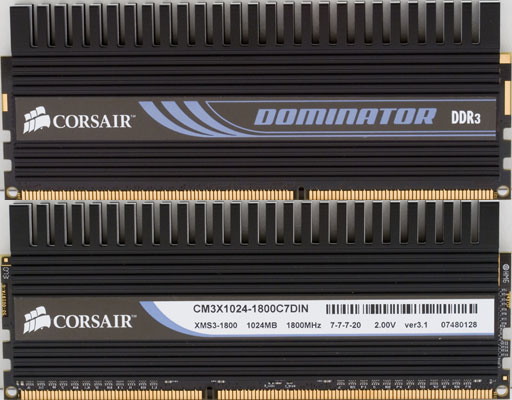
| Module Part Number | 128-145 | - | CM3X1024-1800C7DHX |
| DRAM Manufacturer ID Code | 148, 149 | 00h, 00h | Not specified |
SPD data representation has changed significantly in DDR3 memory modules. First of all, physical characteristics of a module and its memory chips are coded differently. For example, new memory modules specify full size of the array (the number of bits), the number of logical banks and bit capacity of the internal data bus in bits. In order to get the usual form of the memory configuration, full array size (it's 1 Gbit in our case) must be divided by the width of the internal data bus (×8). So it can be written as "256M×8" (or if we take the number of logical banks into account, "32M×8×8 banks", although this form is much more rare). Capacity of a physical bank is more difficult to calculate: chip capacity (in bits) is divided by 8 (to convert bits to bytes), multiplied by the width of the external data bus, and divided by the width of the internal data bus. That's what we get in our case: 1 (Gbit) / 8 (bit/byte) × 64 (bit) / 8 (bit) = 1 GB. As usual, module capacity is calculated as capacity of the physical bank multiplied by the number of physical banks. According to SPD, our modules under review are single-bank products. That's why their module capacity matches bank capacity, that is 1 GB.
Principal changes have been made to representation of all temporal parameters (timings) of memory chips. Instead of using usual nanoseconds to specify cycle time (tCK) and all other timings (except for tCL, we'll discuss it later), DDR3 SPD expresses all parameters in MTB units. The standard also allows to use FTB units (Fine Time Base) probably for fine-tuning some small temporal parameters, about several picoseconds. But DDR3 SPD 1.0 revision does not use them. MTB (as well as FTB) units are specified in nanoseconds as a rational index (dividend : divisor), so it may take up a wide range of values (theoretically—from 255 to 1/255 ns). The default MTB value in the DDR3 SPD standard is 1/8 = 0.125 ns. Another important difference that has to do with temporal parameters is the lack of tCK values corresponding to the main (CL X), reduced(CL X-1), and reduced by two (CL X-2) values of CAS delay expressed in memory bus cycles. Instead, DDR3 SPD contains only tCKmin and CAS latencies (tAAmin), expressed in MTB units (which can be converted to nanoseconds). At the same time, the notion of supported CAS signal durations (expressed in memory bus cycles) is still used by DDR3 SPD. So we can obtain cycle time values corresponding to various tCL values, that is draw analogy to DDR2 SPD data. In our case tCKmin = 1.5 ns, tAAmin = 13.5 ns (9 cycles), supported CAS# values are 9, 8, and 6. These data can be used to represent the following admissible values of cycle time (memory bus frequency) and timings:
| CAS# latency, cycles | 9 | 8 | 6 |
| Cycle time (tCK), ns | 1.5 | 1.6875 | 2.25 |
| Memory bus frequency, MHz (DDR3 speed rating) |
666.7 (DDR3-1333) |
592.6 (DDR3-1185) |
444.4 (DDR3-889) |
| tRCD, cycles | 9 | 8 | 6 |
| tRP, cycles | 9 | 8 | 6 |
| tRAS, cycles | 24 | 21.3 | 16 |
These timing schemes corresponding to "DDR3-1185" and "DDR3-889" modes are of theoretical rather than practical interest. We publish them solely to draw analogy between SPD information in DDR2 and DDR3 memory modules. In our opinion, the "supported CAS latencies" parameter should be excluded. We should keep only the minimum CAS latency (tAAmin) that corresponds to the maximum memory bus frequency (minimum cycle time, tCKmin).
And finally, manufacturer's ID code looks different in JEDEC. Instead of a full 8-byte code with an "honest" sequence of identical continuation codes (7Fh, up to seven codes), we now have an elegant approach with an indication of the number of continuation codes (it's 2 in our case) and manufacturer's ID code (9Eh), which requires only two bytes. The DDR3 SPD standard also includes an SDRAM manufacturer's ID code (for the first time for SPD in DDR memory modules). But in our case the manufacturer did not take this opportunity. Module's manufacturing date, its serial number and part number are specified in a similar way. Our modules under review have only the last piece of info ("CM3X1024-1800C7DHX"), which differs from the one on the label ("CM3X1024-1800C7DIN").
As our modules support XMP, let's examine the contents of this non-standard part of SPD, represented by Bytes 176-254.
| Parameter | Byte(s) | Value | Interpretation |
| XMP ID String | 176, 177 | 0Ch, 4Ah | XMP supported |
| XMP Organization Type | 178 | 00h | Profile 1: disabled (?) Profile 2: disabled |
| XMP Revision | 179 | 10h | Revision 1.0 |
| Medium Timebase (MTB) (dividend : divisor) |
180, 181 | 01h, 09h | 0.111 ns (1 : 9) |
| Profile 1 | |||
| VDD | 185 | 40h | 2.00 V |
| SDRAM Minimum Cycle Time (tCKmin) | 186 | 0Ah | 1.11 ns (900.0 MHz) |
| Minimum CAS Latency Time (tAAmin) | 187 | 46h | 7.77 ns (7 cycles) |
| CAS Latencies Supported (CL) | 188, 189 | 0Ch, 00h | 6, 7 |
| Minimum CAS Write Latency Time (tCWLmin) | 190 | 46h | 7.77 ns (7 cycles) |
| Minimum Row Precharge Time (tRPmin) | 191 | 46h | 7.77 ns (7 cycles) |
| Minimum RAS# to CAS# Delay time (tRCDmin) | 192 | 46h | 7.77 ns (7 cycles) |
| Minimum Write Recovery Time (tWRmin) | 193 | 87h | 15.0 ns (13.5 cycles) |
| Minimum Active to Precharge Delay Time (tRASmin) | 195, 194 | C8h, 10h | 22.22 ns (20.0 cycles) |
| Minimum Active to Active Refresh Delay Time (tRCmin) | 196, 194 | 95h, 10h | 45.0 ns (40.5 cycles) |
| Maximum Refresh Recovery Interval (tREFImax) | 197, 198 | 46h, 00h | 7.77 ms |
| Minimum Refresh Recovery Delay Time (tRFCmin) | 199, 200 | DEh, 03h | 110.0 ns (99 cycles) |
| Minimum Internal Read to Precharge Command Delay time (tRTPmin) | 201 | 44h | 7.55 ns (6.8 cycles) |
| Minimum Row Active to Row Active Delay time (tRRDmin) | 202 | 36h | 6.0 ns (5.4 cycles) |
| Minimum Four Activate Window Delay Time (tFAWmin) | 204, 203 | 0Eh, 01h | 30.0 ns (27 cycles) |
| Minimum Internal Write to Read Command Delay time (tWTRmin) | 205 | 44h | 7.55 ns (6.8 cycles) |
| Temporal optimizations of WRITE-to-READ and READ-to-WRITE commands | 206 | 00h | W-R: by default R-W: by default |
| Temporal optimizations of BACK-to-BACK commands | 207 | 00h | By default |
| System CMD Rate | 208 | 00h | By default |
The contents of the general XMP part includes the XMP support string (present), XMP Revision (1.0), information about profiles (XMP of our modules lacks this information, that is both profiles are sort of disabled, although the first profile actually contains data—perhaps, it happened because the manufacturer used an earlier XMP revision), as well as the MTB value specified in the same way (8-bit dividend and divisor). In our case, this value is reduced to 1/11 = 0.111 ns to make it more convenient to represent other timings.
There is also information about XMP profiles (the first is stored in Bytes 185-219, the second—Bytes 220-254), which are represented only by one (the first) profile in our case. Profile info repeats most of the standard DDR3 SPD part (most timings). Minimum cycle time (tCKmin) equals 1.11 ns (900 MHz memory bus, that is DDR3-1800). Timings (tRCD-tCL-tRP-tRAS) can be represented as 7-7-7-20, which matches characteristics provided by the module manufacturer. There is also a reduced CAS latency value (6), which might correspond to the cycle time of 1.296 ns (approximately 771 MHz, that is "DDR3-1542") and 6-6-6-17.1 timings. However, as in case of the standard DDR3 SPD, it's of little practical interest. Memory voltage specified in this XMP profile also matches the recommended value of 2.0 V.
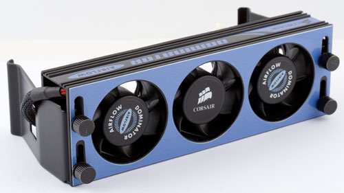
We analyzed memory performance in the standard (certified by JEDEC) DDR3-1600 mode with standard SPD settings and in the unofficial DDR3-1800 mode enabled by the XMP profile. We used the standard voltage of 2.0 V, recommended by the manufacturer (it's higher than the standard voltage by 0.5 V). Memory modules were used with the bundled Airflow cooling system (without fan speed control). We tried to reach the lowest timings possible in both modes.
| Parameter | Testbed 1 | |||
| CPU clock, MHz (FSB clock × FID) |
3200 (400 × 8) |
3150 (450 × 7) |
||
| Memory frequency, MHz (DDR3 mode) |
800 (DDR3-1600) |
900 (DDR3-1800) |
||
| Memory timings, voltage | 9-9-9-24, 2.0 V |
6-6-6-11, 2.0 V |
7-7-7-20, 2.0 V |
7-6-6-13, 2.0 V |
| Average memory read bandwidth, GB/s, 1 core | 7.94 | 8.33 | 9.81 | 9.94 |
| Average memory write bandwidth, GB/s, 1 core | 2.85 | 3.24 | 3.74 | 3.86 |
| Maximum memory read bandwidth, GB/s, 1 core | 9.12 | 9.53 | 11.41 | 11.47 |
| Maximum memory write bandwidth, GB/s, 1 core | 7.31 | 7.31 | 8.22 | 8.22 |
| Average memory read bandwidth, GB/s, 2 cores | 10.65 | 11.33 | 12.72 | 13.02 |
| Average memory write bandwidth, GB/s, 2 cores | 3.06 | 3.40 | 3.75 | 3.82 |
| Maximum memory read bandwidth, GB/s, 2 cores | 11.52 | 12.24 | 13.18 | 13.49 |
| Maximum memory write bandwidth, GB/s, 2 cores | 7.29 | 7.29 | 8.22 | 8.22 |
| Minimum pseudo-random access latency, ns | 26.7 | 25.6 | 21.1 | 21.1 |
| Minimum random access latency*, ns | 66.0 | 59.4 | 51.1 | 49.1 |
| DOOM3 FPS (640×480, low) | 280.1 | 286.4 | 288.5 | 293.2 |
| FarCry FPS (640×480, low) | 441.2 | 451.0 | 463.9 | 463.9 |
*32 MB block size
By default, the ASUS Maximus Extreme motherboard used our memory modules in DDR3-1600 mode at 9-9-9-24 (although this scheme belongs to the DDR3-1333 mode, specified in the SPD by default). FSB clock rate was set to 400 MHz, so the processor operated at 3.2 GHz (400 MHz × 8, so the processor was overclocked by 6.7%). FSB:DRAM = 1:2. We can say that memory operates in the synchronous mode here, characterized by minimum latencies. Theoretical FSB bandwidth in this mode (12.8 GB/s) is twice as low as the theoretical memory bandwidth (25.6 GB/s). Thus, real memory bandwidth values reach 50% of the theoretical performance potential of dual-channel DDR3 memory.
Frankly speaking, we expected even lower results of DDR3-1600 memory on this platform, because our recent analysis of dual-channel DDR2-800 memory on the Intel X48 chipset (which differs from our present Intel X38 only in one thing - its FSB operates at 400 MHz by default, not in the overclocked mode) demonstrated that this platform could reveal the FSB throughput (and dual-channel DDR2-800 memory bandwidth) potential only by 70%. Considering that the bandwidth of the dual-channel DDR3-1600 memory is twice as high, we had expected the real memory bandwidth values to be only 35% of their theoretical maximum.
Nevertheless, real memory bandwidth values published in the table are much higher. It's especially noticeable in maximum real memory read bandwidth in dual-thread memory access mode—about 11.5 GB/s, that is 90% of theoretical FSB throughput (45% of the theoretical bandwidth of DDR3-1600 memory). Extreme timings (our modules under review demonstrated excellent overclocking potential here - 6-6-6-11) increase maximum real memory read bandwidth. In this case, it amounts to 12.24 GB/s in the dual-core access mode, that is over 95% of the theoretical FSB bandwidth. Thus, the reason why the memory potential was not fully revealed in our previous analysis was not in the FSB, but... in DDR2-800 memory itself. To be more exact, in the memory controller of Intel 3 Series chipsets, which cannot use memory bandwidth by 100% in intensive memory access conditions (when a data stream from a processor to the chipset is as heavy as a data stream from the memory controller to system memory). In our case, when a data stream through FSB (from the processor to the chipset) is twice as small as a data stream from system memory to the memory controller (that is memory bandwidth usage does not exceed 50%), the memory controller manages to provide necessary data in time.
The same applies to the DDR3-1800 mode, when the FSB clock rate is increased to 450 MHz (CPU clock rate is 450 MHz × 7 = 3.15 GHz, which means that the CPU is overclocked by 5%), and the memory bus clock rate grows to 900 MHz (the FSB:DRAM ratio remains on the old level, 1:2). In this case, theoretical FSB bandwidth grows to 14.4 GB/s, and theoretical memory bandwidth grows to 28.8 GB/s. Maximum real memory read bandwidth in dual-thread access mode with default timings (7-7-7-20 from the XMP profile) amounts to 13.2 GB/s, which corresponds to 92% of the FSB throughput. When timings are reduced to the minimum possible level of 7-6-6-13, this value is increased to 13.5 GB/s, that is 94% of the theoretical FSB throughput.
It must be noted that lower timings and a faster FSB result in noticeably lower latencies for random memory access. In the first case, random memory access latency is reduced by 10%, when the standard 9-9-9-24 timings are lowered to 6-6-6-11. If we increase FSB and DRAM clock rate by 12.5%, memory latencies drop more noticeably—by 23% (in case of the standard timings) and 17% (with "extreme" timings).
Corsair DOMINATOR TWIN3X2048-1800C7DFIN G memory modules are reliable representatives of the new DDR3 memory generation. They managed to operate with the lowest possible timings scheme (6-6-6-11) at 2.0 V in the fastest DDR3-1600 mode, certified by JEDEC. What concerns the unofficial DDR3-1800 mode, we managed to reduce 7-7-7-20 timings recommended in by XMP to 7-6-6-13.
Real memory bandwidth values in both cases (in DDR3-1600 and DDR3-1800 modes) reached almost 95% of the theoretical maximum of FSB throughput, which acts here as the main memory bottleneck. In other words, these DDR3 memory modules can squeeze maximum memory performance on a given platform (Intel Core 2 processors, Intel 3 Series chipsets). You won't get this effect with DDR2-800 memory modules on this platform, even though it must be theoretically possible. This fact certainly justifies the use of faster memory modules (including DDR3) today with the current generation of Intel platforms.
Write a comment below. No registration needed!
|
Article navigation: |
| blog comments powered by Disqus |
| Most Popular Reviews | More RSS |
 |
Comparing old, cheap solutions from AMD with new, budget offerings from Intel.
February 1, 2013 · Processor Roundups |
 |
Inno3D GeForce GTX 670 iChill, Inno3D GeForce GTX 660 Ti Graphics Cards A couple of mid-range adapters with original cooling systems.
January 30, 2013 · Video cards: NVIDIA GPUs |
 |
Creative Sound Blaster X-Fi Surround 5.1 An external X-Fi solution in tests.
September 9, 2008 · Sound Cards |
 |
The first worthwhile Piledriver CPU.
September 11, 2012 · Processors: AMD |
 |
Consumed Power, Energy Consumption: Ivy Bridge vs. Sandy Bridge Trying out the new method.
September 18, 2012 · Processors: Intel |
| Latest Reviews | More RSS |
 |
Retested all graphics cards with the new drivers.
Oct 18, 2013 · 3Digests
|
|
Added new benchmarks: BioShock Infinite and Metro: Last Light.
Sep 06, 2013 · 3Digests
|
|
Added the test results of NVIDIA GeForce GTX 760 and AMD Radeon HD 7730.
Aug 05, 2013 · 3Digests
|
 |
Gainward GeForce GTX 650 Ti BOOST 2GB Golden Sample Graphics Card An excellent hybrid of GeForce GTX 650 Ti and GeForce GTX 660.
Jun 24, 2013 · Video cards: NVIDIA GPUs
|
|
Added the test results of NVIDIA GeForce GTX 770/780.
Jun 03, 2013 · 3Digests
|
| Latest News | More RSS |
Platform · Video · Multimedia · Mobile · Other || About us & Privacy policy · Twitter · Facebook
Copyright © Byrds Research & Publishing, Ltd., 1997–2011. All rights reserved.