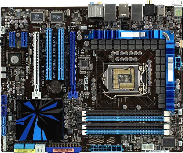
We have already reviewed a couple of ASUS P7P55D motherboards based on the P55 chipsets, and we'll review a few based on the integrated H55/H57 in the near future. This time we got another P55-based product, P7P55D-E Premium. What's so interesting about it? The "E" suffix stands for an updated series. The company has actually re-released most motherboards of the series, having added the support for USB 3.0 and SATA 6Gb/s. Enters the top-class motherboard of the "second wave".
SATA 6Gb/s, USB 3.0
Actually, the preceding P7P55D Premium does support SATA 6Gb/s (unlike all other motherboards of the "first wave") and has wiring layout for a USB 3.0 controller (we don't know why ASUS has had a second thought). Being a top-class model, P7P55D Premium has initially been planned to have full-fledged support for SATA 6Gb/s to squeeze the maximum possible speed from the only controller available back then. The matter is that Marvell 88SE9123 can only be connected to a single PCIe lane. Being unable to do anything about that, ASUS could at least connect it to a PCIe 2.0 lane to provide 500/500 MB/s throughput instead of the 250/250 MB/s of PCIe 1.1.
So how does one get PCIe 2.0 support in case of motherboards based on modern Intel chipsets? As you know, P55/H55/H57 chipsets offer 8 PCIe lanes which are formally PCIe 2.0-compliant, but actually provide only 250/250 MB/s throughput that corresponds to PCIe 1.1.
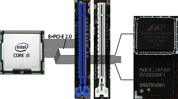
Inexpensive motherboards of the second wave usually suggest that you sacrifice the speed of the PCIe x16 slot and configure CPU (which contains PCIe 2.0 controller) to support two graphics slots in an x8+x8 configuration. Then 8 PCIe 2.0 lanes are used to connect high-speed peripheral controllers. By the way, USB 3.0 is another reason to sacrifice some graphics card performance. Actually, you'll feel a slight decrease in performance, only if you have a high-end graphics card.
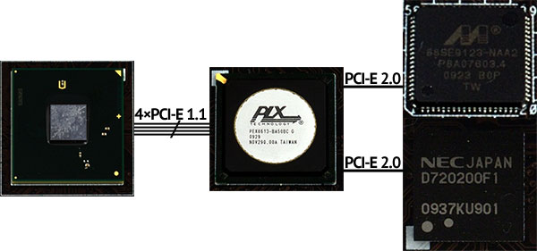
As for P7P55D Premium, and now P7P55D-E Premium, a more elegant solution is used (see the image below). Controllers are connected by means of chipset lanes. The trick is that four PCIe 1.1 lanes are connected to a PLX PEX 8613 switch, the other two ports of which provide a full-fledged PCIe 2.0 lane each.
Whether you really need the throughput offered by the new peripheral standards is another matter. But at least, if you have an ASUS P7P55D/-E Premium motherboard, you can be sure that you get 500 MB/s of bandwidth in each direction.
As for specific controllers that may be used in motherboards, the choice is quite limited, because only one SATA 6Gb/s and one USB 3.0 family has been certified so far. We're talking about NEC µPD720200 (USB 3.0) and Marvell 88SE9123 (SATA 6Gb/s) which are used in this and other motherboards. Well, they could've used a RAID modification of Marvell's controller that provides two SATA-600 ports, but that would've probably looked like outright mockery.
Design
Considering the aforementioned difference in USB 3.0 implementation, P7P55D Premium and P7P55D-E Premium are completely identical. Moreover, the novelty is very similar to the previously reviewed P7P55D Deluxe. The changes in layout and functionality are only dictated by the use of that PCIe switch and the corresponding reallocation of chipset's peripheral lanes. As a result, this motherboard only has two PCIe x16 slots. Egad. But there's nothing they can do about it, because the remaining 4 lanes are barely enough to connect other peripheral controllers and two PCIe x1 slots.

Despite all of the above, the PCB layout is quite ordinary. ASUS sacrificed the seventh expansion slot (not enough lanes) and slightly moved the CPU and memory sockets to the freed space in the center. Next, the right edge features extreme overclocker's voltage controls, CPU power connector and a connector for TurboV Remote. Using these may not be very convenient, especially if you consider CPU power circuitry heatsinks. But, luckily, most users only mess with those once.
The motherboard is moderately conservative, offering two PCI slots, an IDE port and even a COM-port bracket. They decided to go without FDD, though. The horizontal SATA and PATA connectors, as well as a low, wide chipset heatsink, allows installing any expansion cards and connecting any cables.
The PCB also has space for a few convenient trifles called to make your life easier. DIMM sockets only have latches on the one side to simplify installation of memory modules and to save some space. Buttons on the edge of the motherboard allows you to quickly power on or reset the system when you're building or testing your machine. And there's also a Clear CMOS button on the rear panel.
Four LEDs (CPU, memory, graphics card and bootable drive) will help you diagnose possible bootup issues.
Moreover, the motherboard supports the proprietory MemOK! feature. If memory modules refuse to work with the current BIOS settings, push the button to test every possible configuration instead of clearing CMOS.
The motherboard's bundle features an interesting TurboV Remote (which remoteness is kinda limited by its cable length) that controls proprietary utilities. We have already described it in the review of P7P55D Deluxe. Naturally, P7P55D-E Premium supports a top-class variant of the Express Gate feature -- Express Gate SSD with an onboard SSD drive. As you may remember, Express Gate can boot to a special Linux-based Splashtop environment instead of the primary OS. This takes some 5-10 seconds and enables you to browse the Web, use instant messaing, Skype, etc. You can read more on minor pros and major contras of this feature in our review of P5Q Deluxe.

The motherboard features a top-class CPU VRM with 48 "hybrid lanes," whatever that means. The scheme is 32 lanes for the CPU core + 3 lanes for the uncore logic, including the memory controller. That and some dubious improvements provided by the T.Probe feature. Managed by a dedicated controller, the latter, theoretically, balances out load on (and temperature of) different PWM power converter lanes. Since ASUS doesn't provide any implementation details, not to mention any manuals or guides, we can only judge about T.Probe by confusing visualization provided by a propietary utility of the same name. Not quite impressive.
Speaking of actual circuitry, as seen on the PCB, we can say that the PWM controller uses 16 lanes for the CPU core, but its scheme is more complex than usual with two chokes and three FETs per lane. (The uncore power converter has one choke and two FETs per lane.) Anyway, even this simpler 16-lane scheme is definitely sufficiently/excessive complex. And the real meaning of this reducing VR implementation is to attract and hypnotize inexperienced buyers by the magic of numbers, not to reduce voltage ripple under maximum load during extreme CPU overclocking. This is like the digital camera megapixel race.
Marketing aside, there's nothing bad to say about the converter. Just the opposite, the number of lanes guarantee voltage stability under load. Besides, all capacitors are polymer solid, of Nichicon make; FETs are RDS(ON); chokes have ferrite cores.
Write a comment below. No registration needed!


