 |
||
|
||
| ||
|
||
|
||
| ||
Not long ago AMD announced new Phenom X4 processors, based on the new architecture called "AMD Family 10h Processors" (codenamed "AMD K10," previously known as "AMD K8L"). Here is the list of its key features taken from the official documentation (Software Optimization Guide for AMD Family 10h Processors, Publication #40546) versus the architecture of older AMD K8 products.
Our testlab received an engineering sample of the AMD Phenom X4 9700 2.4 GHz, which we already tested in our recent review devoted to efficiency of using memory bandwidth. This review already touched upon some architectural aspects of the new generation of AMD processors. In particular, those that have to do with its L1-L2 bus. In this article we shall analyze the aforementioned key features of the new CPU architecture. We'll compare them with characteristics of a typical AMD K8 processor - Athlon 64 X2 5200+ for the AM2 platform (or, officially, NPT, New Platform Technology). Testbed configurationsTestbed #1: AMD AM2
Testbed #2: AMD AM2+
CPUID characteristicsWe'll start our analysis of the new CPU architecture from AMD with brief CPUID characteristics of a processor, published in Table 1. Table 1. Phenom X4 CPUID
So, it's an AMD processor of the new family 16 (10h), called "Family 10h". Model (2) and stepping (2) numbers correspond to Core Revision B2. Cache and TLB descriptors can be fully unscrambled using the existing documentation (BIOS and Kernel Developer's Guide (BKDG) For AMD Family 10h Processors, Publication #31116). What concerns processor enhancements, we can mention support for MONITOR/MWAIT instructions in addition to SSE3 extensions, available in the latest models of Athlon 64 X2 processors, advanced bit manipulation instructions (POPCNT, LZCNT), SSE4A extensions (SSE4 from AMD, supported instructions are listed in Table 1), and unaligned SSE mode (SSE operations with data, unaligned by the natural 16-byte border). Real Bandwidth of Data Cache/MemoryLet's proceed to test results of the new processor. As usual, we'll start with tests of real bandwidth of all data cache levels and system memory. 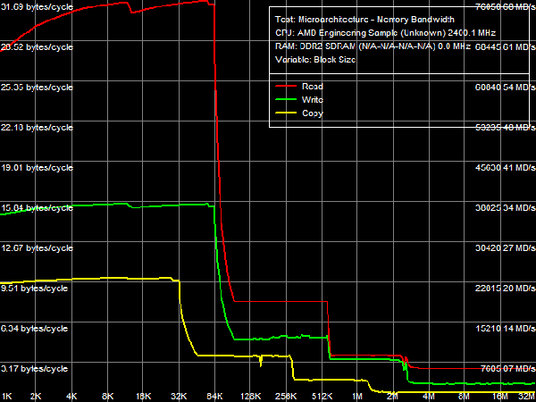 Picture 1. Average Real Bandwidth of Data Cache/Memory, SSE2 The most illustrative results are obtained with 128-bit data access using SSE/SSE2 instructions (see Picture 1). We can clearly see the three-level exclusive architecture of Data Cache. L1-D Cache size is 64 KB (the first inflection). The second inflection at 576 KB corresponds to the total size of L1+L2 caches (64 + 512 KB). And finally, the last inflection at 2.5 MB corresponds to the total size of all cache levels (64 KB + 512 KB + 2048 KB = 2624 KB). Interestingly, L3 cache of the processor, which belongs to the area of its integrated memory controller and is shared between all four cores, is completely captured by the first core in this test, which executes the code and accesses data. We'd also like to note that speed characteristics of L3 Data Cache, especially for reading, are not much higher than those of system memory - you can see it even on a qualitative level - pay attention to the relatively weak inflection on the corresponding curve between L3 Cache and system memory. On one hand, it may speak of high efficiency of the memory controller (which is proved by results of our recent analysis), hardware prefetch from memory in particular. On the other hand, it may indicate low efficiency of data exchange between L3 Cache of the memory controller and a separate processor core. Table 2
*Percent of the theoretical peak memory bus bandwidth is in parentheses. We are more interested in quantitative evaluation of cache bandwidth versus characteristics of the Athlon 64 X2 (a typical representative of the AM2 platform), published in Table 2. The biggest differences between these processors can be seen in L1 data cache bandwidth. In case of 64-bit access with MMX registers, bandwidths of this cache level in Phenom X4 and Athlon 64 X2 are practically identical (~15.7 bytes/cycle for reading, ~8.0 bytes/cycle for writing). However, 128-bit access with SSE or SSE2 instructions changes the situation cardinally: L1 cache bandwidth for reading in the new processor has grown from 8.0 bytes/cycle to ~31.7 bytes/cycle (i.e. it's practically quadrupled!), and its bandwidth for writing has grown from 8.0 bytes/cycle to ~15.7 bytes/cycle (approximately twice as high). Let's try to determine the reasons for these differences (and the lack of such differences in case of 64-bit data access). According to the documentation, L1 data cache of the new Phenom processors has two 128-bit ports (versus two 64-bit ports in L1 Cache of Athlon 64 processors). LSU (Load-Store Unit) can perform two 128-bit read operations or two 64-bit write operations per cycle (a 128-bit write operation is split into two 64-bit operations). Thus, peak bandwidth of the group "CPU registers - L1 D-Cache" can reach 256 bit (32 bytes) per cycle for reading and 128 bit (16 bytes) per cycle for writing. Corresponding speed characteristics of Athlon 64 processors are limited to two 64-bit read operations (128 bit or 16 bytes/cycle) or two 64-bit write operations (128 bit or 16 bytes/cycle). However, we don't have enough data to explain the real bandwidth values demonstrated in our test - only Phenom X4 demonstrates nearly maximum possible results, and it happens only with SSE/SSE2, not in any other case. In order to explain this fact, we should have a look at maximum execution speed of MMX and SSE/SSE2 data load/unload instructions demonstrated by both processors. Athlon 64 processors can execute up to two MMX data load instructions (MOVQ reg, [mem]) and one data unload instruction (MOVQ [mem], reg). Only one SSE/SSE2 data load/unload instruction (MOVAPS or MOVDQA) can be executed per two cycles. It explains our L1 Cache bandwidth values obtained in such processors: two MMX instructions for reading data provide the read bandwidth of 16 bytes/cycle, one MMX instruction for writing - write bandwidth of 8 bytes/cycle, and execution of SSE/SSE2 instructions at the speed of one instruction per two cycles limits the real bandwidth of L1 Cache to 8 bytes/cycle both for reading and writing. The situation with new Phenom processors is different. Bit capacity of their FP execution units (they process all SSE/SSE2 instructions, even those that don't have to do with computing) was expanded to 128 bit. The core of these processors can execute SSE/SSE2 instructions at impressive speed - up to 2 load instructions per cycle (FADD and FMUL pipes) and up to one unload instruction per cycle (FSTORE pipe). Execution speed of MMX instructions remains the same as in the Athlon 64 processors. Thus, execution units and L1 cache in these processors work in coordination, as they transfer data: two 128-bit ports of L1 Cache/LSU provide bandwidth (256 bit or 32 bytes/cycle) that equals maximum execution speed of SSE/SSE2 read instructions (two per cycle); what concerns writing, execution of up to two 64-bit data transfer operations from LSU to L1 Cache (128 bit or 16 bytes/cycle) corresponds to maximum execution speed of SSE/SSE2 write instructions (one per cycle). Let's analyze L2 D-Cache bandwidth, which has grown much in new processors - almost twofold for reading (7.66-7.98 bytes/cycle versus 4.02-4.10 bytes/cycle) and approximately by 25-30% for writing (4.94-5.10 bytes/cycle versus 3.92-3.94 bytes/cycle). We already noted in our first review, devoted to efficiency of memory operations in new processors, that the effective width of L1-L2 cache bus for reading grew to 128 bit, which is proved by test results. Bandwidth values of L3 Cache in Phenom processors are not much lower than bandwidth values of L2 Cache in the previous generation of Athlon 64 X2 processors - even though L3 Cache is not part of a CPU core, while L2 Cache in Athlon 64 and Phenom processors is integrated into the core. We can assume that bit capacity of the L2-L3 bus is 64 bit (we'll verify this assumption later), that is it equals bit capacity of the L1-L2 bus in Athlon 64 processors. What concerns memory bandwidth, we've recently shown that it has grown much relative to Athlon 64 X2 for reading, remaining approximately on the same level for writing. On one hand, it can be explained with a significantly increased bandwidth of the L1-L2 bus. On the other hand, it may be the effect of higher efficiency of hardware prefetch from memory in Phenom processors. However, it should be noted that the real memory bandwidth value is below 50% of the theoretical bandwidth of dual-channel DDR2-800 memory (memory controller was operating in ganged mode, which provides this very theoretical memory bus bandwidth even for "single-core" access). Besides, L3 Cache bandwidth for reading data from a single core (approximately 3.7 bytes/cycle, that is about 8.9 GB/s) is also below the theoretical bandwidth of dual-channel DDR2-800 memory. It proves our assumption (made in the previous review) about limited efficiency of the integrated memory controller per core, which can be avoided with multi-core memory access. Maximum Real Memory BandwidthLet's evaluate maximum real memory bandwidth in a single core access mode obtained with optimized read (software prefetch) and write (non-temporal store) operations. 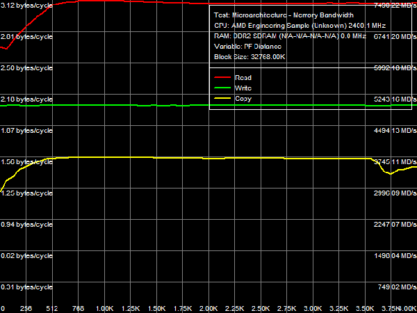 Picture 2. Maximum real memory bandwidth, SSE2, Software Prefetch/Non-Temporal Store Test results are published in Picture 2 and Table 3. Efficiency of software prefetch reaches its maximum with the PF distance of 768 bytes and higher. However, its efficiency is quite low - memory bandwidth reaches ~7.5 GB/s (58.5% of the theoretical memory bandwidth), only 17% faster than in the usual read mode. For your information, efficiency of software prefetch in Athlon 64 X2 processors is much higher - it doubles memory bandwidth. It most likely has to do with high efficiency of hardware prefetch in Phenom processors, it's so good that software prefetch has nothing to do, it becomes sort of redundant. It was especially noticeable in our recent analysis of DDR2-800/DDR2-1066 memory bandwidth utilization in case of "multi-core" memory access. We can only add that high efficiency of hardware prefetch, which makes software prefetch redundant, is a great advantage of the new processor architecture from AMD - software developers can forget about software prefetch (calculating a PF distance and inserting PREFETCHx instructions) in their code. At the same time, we are disappointed with maximum real memory bandwidth results for writing, it indicates a weak implementation of non-temporal store (when no cache is used). It amounts to 39% of the theoretical memory bandwidth and approximately 69% of the results demonstrated by Athlon 64 X2. We can assume that the problem is in L3 Cache of the processor, shared for all cores, which is integrated into the north bridge. This method organizes a direct data channel from a processor core into system memory, evading the north bridge. Table 3
*Percent of the theoretical peak memory bus bandwidth is in parentheses. Average Latency of Data Cache/MemoryLet's proceed to D-Cache/Memory latency tests, which can detect new interesting peculiarities of the AMD Phenom architecture. 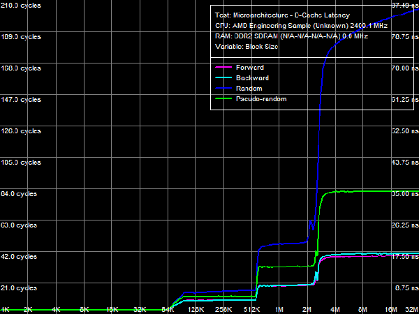 Picture 3. Data Cache/Memory Latency Qualitative test results (Picture 3) match those of the memory bandwidth test for various cache levels in terms of their size and organization type (exclusive). However, latencies of all cache levels, but L1, differ depending on a memory access mode (forward, backward, pseudo-random, or random). It indicates that hardware prefetch is organized on all cache levels (from L2 Cache, L3 Cache, and system memory) for the first time in AMD processors (all previous generations of AMD K7 and K8 processors featured hardware prefetch only from system memory). Table 4
Quantitative results are published in Table 4. Average latency of L1 D-Cache in the new processors remains on the level of three cycles. Average latency of L2 Cache depends on an access mode: it's about nine cycles for forward and backward walks (when hardware prefetch is maximum efficient), approximately 14.5 cycles for random walks, pseudo-random results are somewhere in between (approximately 12 cycles), which indicates that hardware prefetch can work well even in this case. The corresponding value in Athlon 64 X2 processors does not depend on a walk mode and amounts to about 17 cycles. There is a similar situation with average latencies of L3 Cache: it's minimal (~19.5 cycles) for forward and backward walks, and it's maximal for random (~47.5 cycles) walks. Pseudo-random walks show intermediate results. And finally, the same concerns system memory, but with a wider spread: average memory latencies vary from 16-17 ns to 85 ns. The growing random access latency has to do with the increasing number of L2 D-TLB misses, which size is 512 entries, 4-KB pages. That is it can cover up to 2 MB of random memory calls (the corresponding inflection on the curve is not noticeable, because it overlaps the L3 Cache size inflection). Minimum D-Cache/Memory LatencyLet's evaluate minimum latencies of different D-Cache levels. It looks like a piece of cake, but hardware prefetch on all levels makes this task much harder. 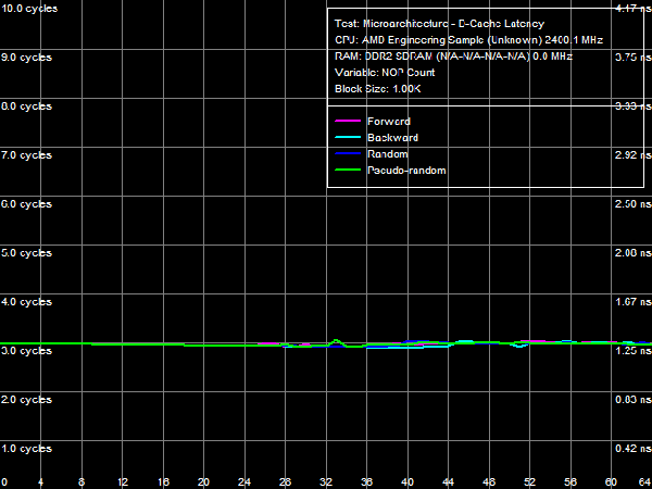 Picture 4. Minimum L1 Cache Latency L1 D-Cache is the easiest case, its latencies are published in Picture 4. It equals the average latency of this cache level, 3 cycles (see Table 5). 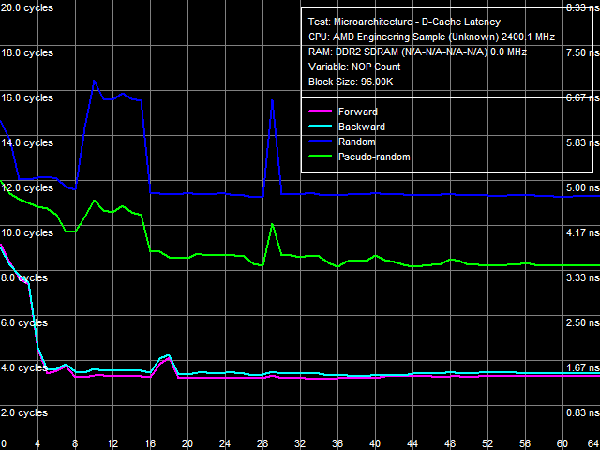 Picture 5. Minimum L2 Cache Latency, Method 1 An attempt to evaluate minimum latency of L2 Cache in the same way does not yield good results - the situation is complicated by hardware prefetch (see Picture 5). It offloads L2 Cache completely already with five NOPs (no cache access) between two calls, and its latency is reduced practically to the level of L1 Cache, approximately 3.3 cycles. Pseudo-random walks require 16 NOPs, and the minimum latency is approximately 8.2 cycles. Random walks require no less than 30 NOPs to offload the cache, and the minimum latency is 11.5 cycles - it's the closest result to what we expected after reading the documentation (9 additional cycles of latency versus L1, that is the total latency is 12 cycles). 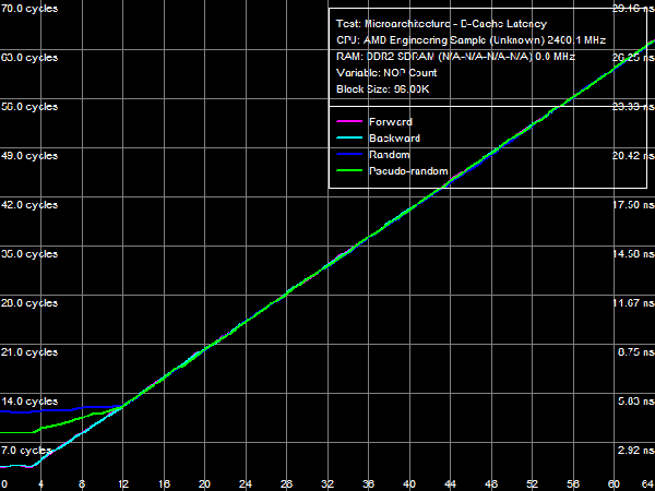 Picture 6. Minimum L2 Cache Latency, Method 2 Let's evaluate minimum latency of L2 Cache and obtain its real value using Method 2 (see Picture 6). It was initially developed for processors with speculative data loading (Intel Pentium 4 Prescott and older products). A measure of latency in this method is the number of NOPs used to offload the bus (which produce an inflection on the curve) multiplied by their execution speed in the dependent chain of instructions (it's one instruction per cycle in our processors under review). Inflections on forward, backward, and pseudo-random curves can be seen at three NOPs, that is the minimum latency of these levels equals L1 latency (3 cycles) owing to hardware prefetch. Only random walks give correct values of L2 latency without prefetch - the inflection on the corresponding curve is at 12 cycles. Interestingly, all four curves cross at the point of 12 NOPs. We'll show below that this point can be a more reliable criterion of reaching true latency of a given data cache level. 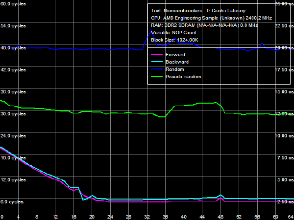 Picture 7. Minimum L3 Cache Latency, Method 1 We'll try to evaluate minimum latency of L3 Cache in Phenom processors by analogy with L2 latency tests. We'll use a modified test of "Minimal L2 D-Cache Latency, Method 1/Method 2", by increasing the block size from 96 KB to 1024 KB (to get into L3). Results of this test (Method 1) are published in Picture 7. In much the same way, forward and backward walks need 24 or more NOPs to offload L3 Cache, which leads to its minimum effective latency of 5.0-5.5 cycles. However, the bus practically cannot be offloaded in case of pseudo-random walks, and minimum latency (~28.2 cycles) does not differ much from its average value (~32 cycles). The same can be said about the random access mode, when the minimum latency is approximately 46.7 cycles. 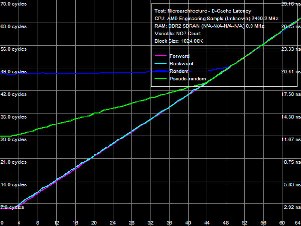 Picture 8. Minimum L3 Cache Latency, Method 2 Let's try Method 2 to get a more accurate value of L3 latency. Its results are published in Picture 8. As in case of L2 Cache, hardware prefetch equals the effective L3 latency for forward, backward, and pseudo-random walks to L1 latency (3 cycles). Theoretically, this result is correct - in case of absolutely efficient hardware prefetch (and completely offloaded data bus) all requested data will be in L1 Cache, and the effective latency will equal latencies of this cache level. Besides, an inflection in the random access curve (when efficiency of hardware prefetch is close to zero) is quite indistinct - this curve gradually grows with the number of NOPs, there is a surge at 44-48 NOPs. In this very case the cross point of all curves is a more reliable criterion of real L3 latency, at about 48-49 NOPs. Considering the above data on average L3 latency, real latency of this cache level is 48 cycles (B±1 cycle). 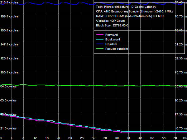 Picture 9. Minimum Memory Latency In conclusion, we are going to evaluate minimum memory latency of the Phenom X4 platform. Like in all above-mentioned cases, hardware prefetch reduces it to very low values for forward and backward walks (4.6-5.4 ns, that is just 11-13 cycles). However, minimum latencies demonstrated in pseudo-random and random walks are practically on the level of average latencies. On the contrary, offloaded L2-RAM bus on the Athlon 64 X2 platform reduces random access latency (from 86 ns to 74 ns, that is approximately by 14%). Table 5
Data Cache AssociativityAssociativities of all three cache levels (L1-D, L2, and L3) are known from CPUID characteristics: they amount to 2, 16, and 32 cycles correspondingly. So the real situation with associativity, published in Picture 10, looks especially interesting. 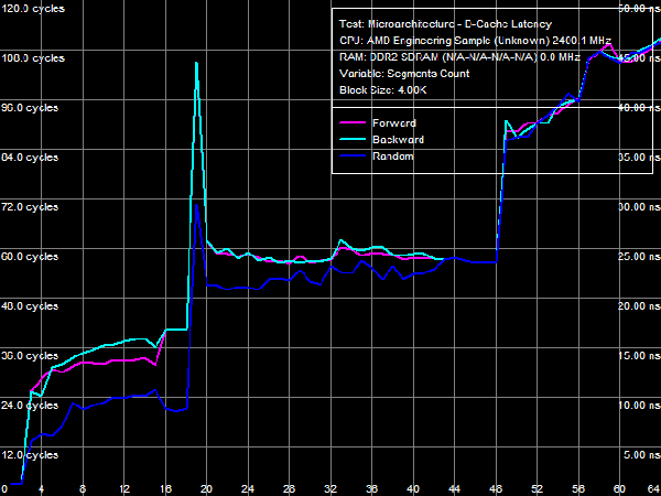 Picture 10. Data Cache Associativity The first inflection can be seen at 2 cache segments (segment size in this test equals 1 MB) and corresponds to L1 D-Cache associativity. The second inflection appears when 18 cache segments are exceeded, which is typical of exclusive cache organization - it corresponds to the total associativity of L1-D and L2 Caches (2+16). But the most interesting inflection is the last one at 48 cache segments. By analogy, it must correspond to the total associativity of all three cache levels, which should actually be 50 (2+16+32). This test shows that L3 associativity is just 30. It's not quite clear why it happens. However, it may have to do with peculiarities of L3 localization (in the memory controller, not in the processor core) and consequent sharing of this cache level by all processor cores. L1-L2 Cache Bus Real BandwidthWe've already touched upon this architectural detail of new Phenom processors in our first article devoted to the analysis of the memory system in the new platform, as it's very important for effective utilization of high bandwidth of dual-channel DDR2-800/DDR2-1066 memory. 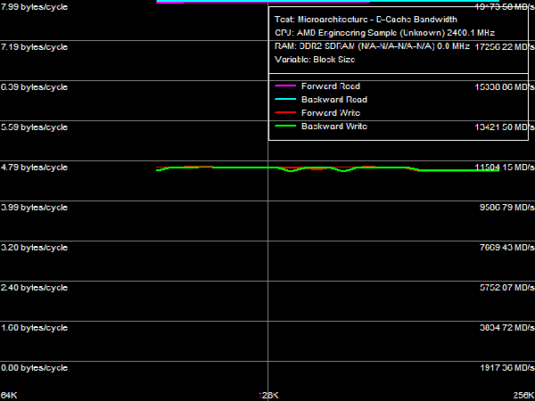 Picture 11. L1-L2 Cache Bus Real Bandwidth Test results of the real L1-L2 bus bandwidth are published in Picture 11, and its quantitative comparison with the Athlon 64 X2 is given in Table 6. Table 6
Full width of L1-L2 bus in Athlon 64 processors is 128 bit. But it's organized as a 128-bit bidirectional bus (in other words, it consists of two 64-bit buses), so we get only 64 bit in one direction. Its full bit capacity can be demonstrated in this test, which quantitative results must be multiplied by two to take into account the exclusive cache organization (when a line is sent from L2 to L1 cache, a line is pushed out of L1 into L2). Thus, L1-L2 cache bandwidth for reading cache lines is about 9.34-9.70 bytes/cycles, that is 58-61% of the theoretical value. Bandwidth of this bus for writing cache lines is a tad lower, ~9.10 bytes/cycle, that is 57% of the theoretical bandwidth. Test results show that full width of the L1-L2 bus in new Phenom processors is also 128 bit (its maximum bandwidth is 16 bytes/cycle). However, efficiency of its utilization has grown significantly. For example, bandwidth of this bus for reading cache lines reaches almost the maximum value (15.96-15.98 bytes/cycle). However, bandwidth of this bus for writing cache lines hasn't grown much, it's 9.34-9.42 bytes/cycle (58-59% of the theoretical value). For a deeper analysis of L1-L2 bus organization we are going to use the data arrival test (#1), which results are published in Picture 12. 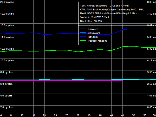 Picture 12. Data Arrival Test 1 on L1-L2 Cache bus As hardware prefetch is present on all cache levels, results of this test for forward and backward walks (and pseudo-random, to some degree) are not reliable. In case of random walks, the total latency of two calls to elements of the same line in L2 Cache in the 2nd DW offset area is about 14-14.5 cycles (the theoretical value is 15 cycles, the sum of L1 and L2 latencies). With the 2nd DW offset of 48 bytes and more, it grows by one cycle. That is the maximum amount of data that the L1-L2 bus can transfer without delays within L1 access times (3 cycles) is 48 bytes. Hence, maximum bandwidth of this bus in one direction is 48/3 = 16 bytes/cycle (128 bit). Considering that its full bit capacity is also 128 bit (as we have shown above), we can say that the L1-L2 D-Cache bus in Phenom processors is a unidirectional 128-bit bus. The same bus organization, but twice as narrow, is used in AMD Athlon (K7) processors. There also exists a different interpretation of these test results. The 128-bit capacity per direction is proved by the data arrival test (#1). But we can assume that its full capacity can still be 256 bit, that is it's a bidirectional bus (two 128-bit buses), similar to the L1-L2 bus in Athlon 64 processors, but twice as wide. For unknown reasons, its efficiency for reading/writing cache lines is twice as low as in the previous test, that is 50% for reading cache lines and 29% for writing cache lines. Unfortunately, we found no real proof of this assumption. It can be justified only from the point of view of common sense (evolution of a bidirectional bus in AMD K8 looks more logical than the return to a unidirectional bus in AMD K7). Besides, in this case we'll have to explain why its real bandwidth falls within the theoretical bandwidth of a 128-bit bus and does not exceed half of the 256-bit bus bandwidth (while the real bandwidth of the L1-L2 bus in processors of the previous generation with the same bus organization reaches 60% of the theoretical maximum). 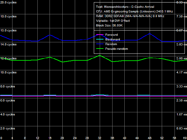 Picture 13. Data Arrival Test 2 on L1-L2 Cache Bus Let's analyze results of the Data Arrival Test 2 on the L1-L2 bus, where a variable value is the 1st DW offset. This test evaluates how a line is read from L2 into L1 - from the very beginning to its end or it's possible to read a part of the line. This test method is described in our first review of AMD K7/K8 processors, so we shall not repeat ourselves here. We can only note that typical peaks on the random access latency curve with 0-, 16-, 32-, and 48-byte offsets mean that a cache line can be read from each 16th byte (for example, in the following sequence of bytes: 32-47, 48-63, 0-15, 16-31). The same happens with AMD K7/K8 processors, but with an 8-byte step. Multiplicity of the step corresponds to bit capacity of the L1-L2 bus in one direction: 64 bit for AMD K7 and K8, 128 bit for Phenom. Real Bandwidth of the L2-L3 BusBy analogy with the L1-L2 bus tests, we shall evaluate bit capacity and performance characteristics of the L2(core)-L3(memory controller) bus. We'll use the same tests with the block size increased from 96-240 KB to 640-2048 KB. 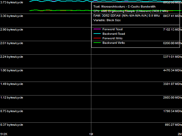 Picture 14. Real Bandwidth of the L2-L3 Bus Results of the real bandwidth test of the L2-L3 bus are published in Picture 14 and Table 7. Table 7
Interestingly, L2-L3 bus bandwidth values per se are very close to values of real bandwidth of L3 cache for reading/writing, obtained in the corresponding test. However, as in case of the L1-L2 bus, test results should be doubled to take into account the exclusive organization of this cache level. Thus, the L2-L3 bandwidth is 7.46 bytes/cycle for reading cache line and 6.92 bytes/cycle for writing them. These test results can again be interpreted in two ways: it's either a 64-bit unidirectional bus with the peak bandwidth of 8 bytes/cycle (the real bandwidth is 86-93% of the theoretical maximum), or it's a 128-bit bidirectional bus (that is a full counterpart of the L1-L2 bus in Athlon 64 processors), which is utilized by just 43-47%. We can choose one of these interpretations only using our common sense - it will be odd to use an older bus implementation. Besides, if we take into account that the L2-L3 bus is actually a data exchange bus between a separate core and an integrated memory controller, it's much more reasonable to assume a bidirectional organization of this bus, which allows to read (from system memory or L3 Cache) and write data (or push data out of L1/L2 Cache into L3 Cache) simultaneously. 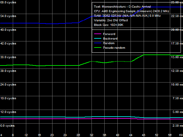 Picture 15. Data Arrival Test 1 on L2-L3 Bus To prove that bit capacity of the L2-L3 bus in one direction is at least 64 bit, we'll use the Data Arrival Test 1. Its results are published in Picture 15. It's difficult to give a quantitative evaluation of this result (pseudo-random and random curves), because latencies grow when the 2nd element is offset by 32 bytes and more, as it must be at the 24-byte offset for the 64-bit bus (8 bytes multiplied by 3 cycles for data access). As we have shown above, if the bus is 128 bit wide in one direction, latency should grow at the 48-byte offset and higher. Thus, bit capacity of the L2-L3 bus in one direction does not exceed 64 bit. I-Cache, Decode/Execute EfficiencyLet's evaluate efficiency of L1 I-Cache (L1-I) and shared L2/L3 I/D-Caches for decoding and executing simple ALU instructions in an independent chain. The most illustrative result from the point of view of L1-I bandwidth for decoding/executing 8-byte CMP prefix instructions ([F3h][67h]cmp eax, 00000000h) is published in Picture 16. 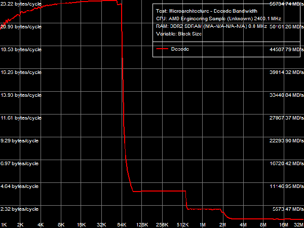 Picture 16. Decode/execute efficiency for 8-byte CMP prefix instructions We can see that the exclusive organization of L1/L2 and L2/L3 Caches also shows itself in caching the stream of instructions (there are inflections in areas corresponding to the total size of L1+L2 and L1+L2+L3 Caches), which looks natural. Maximum real bandwidth of L1-I Cache in this test reached 23.22 bytes/cycle (versus 16 bytes/cycle in Athlon 64 processors, see Table 8). It indicates that the peak bandwidth (bit capacity) of L1 I-Cache as well as L1 D-Cache is 32 bytes/cycle (256 bit). Impossibility to reach such a high theoretical bandwidth of L1-I Cache has to do with limitations of the decoder and ALUs of the processor, which can do only 3 instructions/cycle (in this case it's a tad lower - about 2.9 instructions/cycle, as it's necessary to truncate unnecessary REP (F3h) and Address Override (67h)). Table 8
Quantitative characteristics of L1-I, L2- and L3 bandwidth as well as of CPU execution units are published in Table 8. Decode/execute efficiency for most simple ALU instructions from L1 I-Cache hasn't changed - it's still limited to 3 instructions/cycle, because there are only three ALUs in the CPU core. Yet, as we have already mentioned above, decode/execute efficiency of large instructions like 6-byte CMPs (cmp eax, 32-bit value) and 8-byte prefix CMPs ([F3h][67h]cmp eax, 32-bit value) has grown to its maximum (3.0 and 2.9 bytes/cycle correspondingly), as the L1-I bus is expanded to 256 bit. Execution speed of code from L2 cache has also grown owing to the increased L1-L2 bus bandwidth (maximum real bandwidth of this cache level is 3.78 bytes/cycle versus 3.28 bytes/cycle in Athlon 64 X2). Execution speed of code in shared L3 Cache is approximately 2 bytes/cycle. I-Cache AssociativityLet's evaluate behaviour of L1 I-Cache and Shared L2/L3 I/D-Caches in the I-Cache Associativity test. Test results are published in Picture 17. 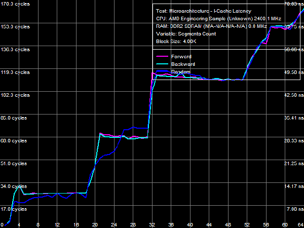 Picture 17. I-Cache Associativity The first inflection is at two segments of cache, it corresponds to L1 I-Cache associativity. The second inflection also corresponds to the official characteristics: it's at 18 segments of cache and corresponds to the total associativity of L1-I and L2 Caches of the processor. The most interesting result has to do with associativity of L3 Cache, shared by all CPU cores. The true (official) associativity of this cache level is 32, while the D-Cache Associativity test shows that L3 associativity is 30 (so we've made an assumption that it happens because L3 Cache is shared by all processor cores, while all our tests are executed by a single core). When a processor executes code, associativity curves show two inflections: the first one is at 32 cache segments (which corresponds to associativity of L3 = 14), the second is at about 50 cache segments, which corresponds to the true associativity of L3 = 32. The reasons of such L3 behavior are not clear, the above assumption is the only sane explanation. TLB CharacteristicsIn conclusion, let's prove that TLB characteristics known from CPUID descriptors are true in real tests. We'll start with tests of D-TLB size and associativity. 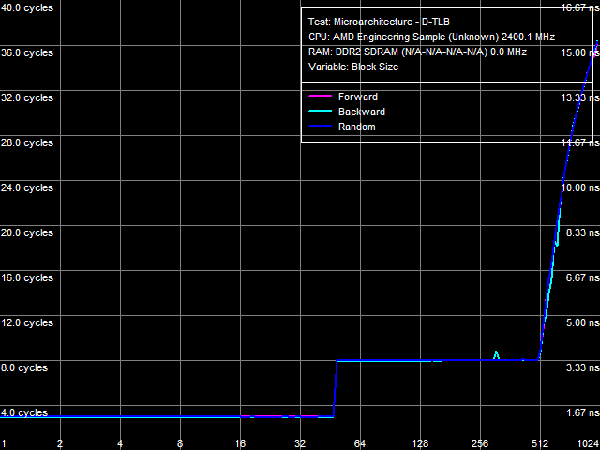 Picture 18. D-TLB Size You can see in Picture 18 that the size of the first D-TLB level is 48 entries (4-KB pages, it's a standard for 32-bit OS), miss penalty for this D-TLB level in all cases is 5 cycles. L2 D-TLB size is 512 entries (which corresponds to 2 MB), miss penalty depends on the number of used memory pages. It's about 28 cycles in case of 1024 pages (4 MB) - a tad higher than in Athlon 64 processors, where the miss penalty is approximately 17 cycles.  Picture 19. L1 D-TLB Associativity  Picture 20. L2 D-TLB Associativity L1 and L2 D-TLB Associativity test results are published in Picture 19 and 20. The first test proves full associativity of L1 D-TLB. The second shows that associativity of L2 D-TLB equals 4, and an associativity miss penalty is approximately 34 cycles (it's higher than a size miss penalty, Athlon 64 processors were in a similar situation). 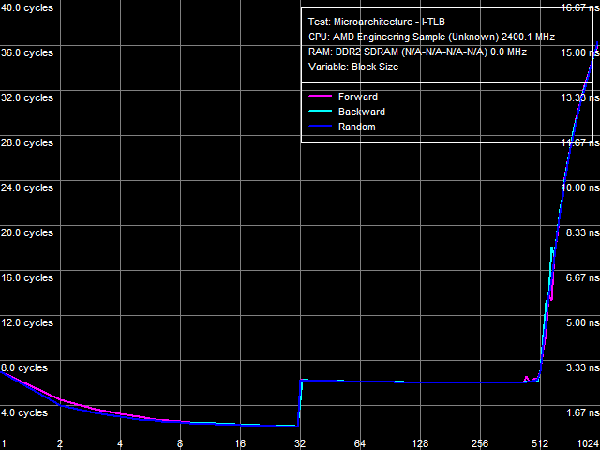 Picture 21. I-TLB Size Results of the I-TLB Size test are published in Picture 21. As in case of D-TLB, we can clearly see a two-level organization of I-TLB. L1 I-TLB size is 32 entries, miss penalty - 4 cycles. L2 I-TLB size is 512 entries, a miss penalty also depends on the number of memory pages. It's about 30 cycles - higher than in Athlon 64 processors (24-26 cycles depending on a CPU). 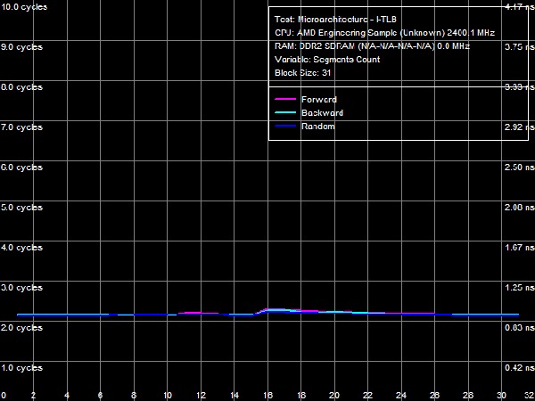 Picture 22. L1 I-TLB Associativity 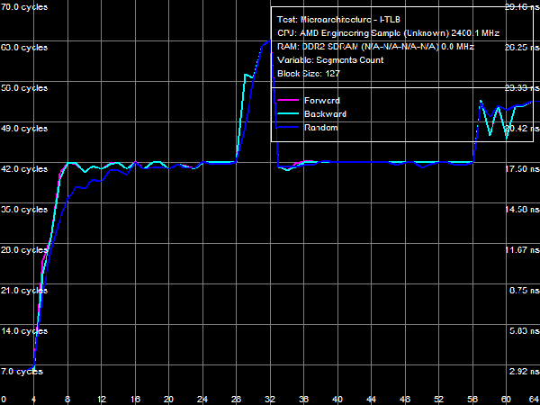 Picture 23. L2 I-TLB Associativity Results of the L1 I-TLB Associativity test, published in Picture 22, show full associativity of this level. Picture 23 proves that L2 I-TLB associativity equals four with an associativity miss penalty of about 36 cycles. ConclusionsThe architecture of new AMD Phenom processors (AMD K10) reviewed in this article is quite successful. Its main advantage over the previous architecture (AMD Athlon 64, K8) is its balanced design on all levels. For example, the L1 D-Cache bus is expanded to 256 bit (2x128) agrees well with 128-bit FP arithmetic units, providing equal bandwidth for reading data using 128-bit SSE/SSE2 multimedia instructions (32 bytes/cycle). And the 128-bit FP units per se can yield a noticeable performance gain in most synthetic and real applications working with this data type (e.g. scientific programs, 3D Modeling, computer games, etc). In our simple case (reading data with 128-bit SSE/SSE2 instructions), their execution speed has grown fourfold. Expanded to 128 bit in one direction, the L1-L2 D-Cache bus (which organizational type is still in question) eliminates a bottleneck in the data exchange process between a processor core and system memory (it's hard to imagine that the L1-L2 bus is as wide as the L2-memory controller bus in AMD K8 processors!) A great advantage of the new architecture is its efficient hardware prefetch on all levels (L2, L3 Caches, and system memory). As we have shown in our separate review, it can show its true worth in case of multi-core access to system memory, reaching up to 85% of performance potential of high speed dual-channel DDR2 memory. What concerns L3 Cache in its integrated memory controller shared for all processor cores, this cache level is not an apparent advantage of new processors. According to our single-core access tests, bandwidth of this cache level is not much higher than bandwidth of system memory in the same conditions (8.9 GB/s versus 6.4 GB/s), which has to do with high bandwidth of dual-channel DDR2 memory. L3 Cache has better latencies, but only for random memory access (in other cases latencies of all levels are effectively "camouflaged" by hardware prefetch). So its advantages can be more noticeable in applications that randomly access data stored in different areas of memory (for example, databases). Dmitry Besedin (dmitri_b@ixbt.com)
February 20, 2008 Write a comment below. No registration needed!
|
Platform · Video · Multimedia · Mobile · Other || About us & Privacy policy · Twitter · Facebook Copyright © Byrds Research & Publishing, Ltd., 1997–2011. All rights reserved. | ||||||||||||||||||||||||||||||||||||||||||||||||||||||||||||||||||||||||||||||||||||||||||||||||||||||||||||||||||||||||||||||||||||||||||||||||||||||||||||||||||


