 |
||
|
||
| ||
|
||
|
||
| ||
Our main review of the new architecture used in AMD Phenom X4 processors already touched upon their bug in L3 Cache TLB, which can freeze the system in experimental conditions (and probably in real conditions, according to the latest info). Our Phenom test results show that the bug does not have to do with L1/L2 D-TLB and/or I-TLB. Perhaps, it really affects some area in the integrated memory controller and/or L3 Cache, which can be called TLB (translation lookaside buffer). But this structure is not officially documented for these processors (and we don't know its characteristics). Anyway, AMD confirms that the bug exists. Motherboard manufacturers are also aware of this bug, so they release new BIOS versions with the patch to fix it. Unfortunately, it cannot be fixed "for free" (to all appearances, the patch disables this "TLB" structure), it reduces system performance by approximately 10-15%. According to some test results that have recently appeared in the Web, this patch can reduce system performance in various real applications (the spread of results is wide, the average performance drop is about 14%). However, the idea that the bug (and the corresponding patch) can affect a processor core, that is its execution units, seems unlikely. System performance is probably reduced because of deteriorated speed characteristics of memory and/or L3 Cache in the integrated memory controller. In order to prove it and to show how exactly the above-mentioned systems change with the patch, we decided to compare low-level characteristics of the AMD Phenom X4 platform with what we already obtained without the patch. Testbed configurationsTestbed 1 (without the patch)
Testbed 2 (patched)
Real Bandwidth of Data Cache/MemoryFirst of all I'd like to note that absolute test results of the patched AMD Phenom X4 published in this review may differ from our older results (obtained without the patch) because of different motherboards used in the testbeds (see testbed configurations). In particular, when we tested the platform for the first time (Testbed 1, MSI K9A2 Platinum motherboard), we didn't know which frequency of the north bridge and L3 Cache were set by default. What concerns the second system analyzed in this article (Testbed 2, Gigabyte MA790GX-DQ6 motherboard), AMD Overdrive detects that the default frequency of the memory controller and L3 Cache is 2.0 GHz, while the core clock rate is 2.4 GHz. It will be reasonable to assume that the same default mode is used by the first motherboard. In this article we've increased the frequency of the north bridge to 2.4 GHz manually in BIOS Setup to ensure synchronous operation of processor cores and the integrated memory controller and to compare this mode with the default one (2.4 GHz CPU, 2.0 GHz NB). Measurements of D-Cache and Memory bandwidths are published in Table 1. Table 1
As we have expected, the patch does not change performance characteristics of L1- and L2- D-Caches. Performance characteristics of L3 Cache in the second testbed grow a little (by 8-11%), while memory performance drops significantly (especially, read bandwidth, approximately by 18%). Results of this test can be used to draw a preliminary conclusion that the patch does not affect L3 Cache much (its bandwidth grows, because its clock rate is increased from 2.0 GHz to 2.4 GHz, although bandwidth gain is smaller than the 20% frequency growth), but it affects memory bandwidth (despite the increased frequency of the memory controller). The lack of influence on L3 Cache will be confirmed by our other tests. Maximum Real Memory BandwidthMaximum real memory bandwidth values of the patched system, published in Table 2, are also lower: maximum real memory bandwidth for reading drops by 19.5%, for writing - by approximately 4.5%. Table 2
*values relative to theoretical memory bus bandwidth limit are in parentheses Average Latency of Data Cache/MemoryLet's proceed to tests of D-Cache and RAM latencies, which can reveal the effect of the patch on the qualitative level (Picture 1).  Picture 1. Average D-Cache/Memory Latency Namely, the effect manifests itself as a surge in random access latency, starting from 2 MB block size, which corresponds to the L2 D-TLB size of the processor core. Thus, this test is an indirect proof that the L2 D-TLB miss penalty grows much, we'll see it in the special D-TLB test. Table 3
Quantitative characteristics of L1-, L2-, and L3-Cache latencies, published in Table 3, show that practically nothing changes with the patch. It again proves that the patch does not affect L3 Cache. The increased memory latencies (approximately by 13% for pseudo-random access and over 2.6 times(!) for random access) prove that memory performance deteriorates significantly when L2 D-TLB misses (that is when these misses should be masked by the undocumented TLB structure of the integrated memory controller, disabled by the patch). Minimum D-Cache/Memory LatencyConclusions on average D-Cache and memory latencies can be applied to minimum latencies as well (Table 4). Note the reduced efficiency of hardware prefetch, which manifests itself in the increased memory latencies for forward and backward walks, although it cannot be a direct result of disabling "TLB" in the integrated memory controller. Table 4
Data Cache AssociativityL1-, L2-, and L3 D-Cache associativity measurements (Picture 2) do not differ from the point of view of cache associativity values. But they demonstrate a significant associativity miss penalty for all cache levels, if more than 48 cache segments are used. This effect is probably related to the L2 D-TLB miss, when memory access latencies should be masked by TLB of the memory controller. 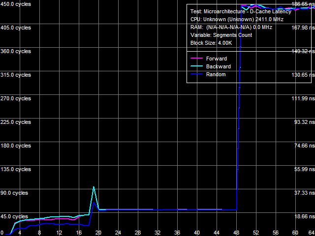 Picture 2. Data Cache Associativity L1-L2 Cache Bus Real BandwidthLike the average real bandwidth of L2 Cache, the patch does not change real bandwidth of L1-L2 bus (see Table 5) either. Table 5
Real Bandwidth of the L2-L3 BusWhat concerns the real bandwidth of L2(processor core)-L3(memory controller) bus, its speed characteristics (see Table 6), just like the previously measured bandwidth of L3 Cache, are a tad higher in the new testbed (approximately by 8%) because of the higher frequency of the integrated memory controller (2.4 GHz versus 2.0 GHz). Table 6
I-Cache, Real Decode/Execute BandwidthThere is apparently no effect of the patch on the decode/execute speed of instructions from L1-I and L2 Caches (see Table 7). Yet, execution speed of code from L3 Cache grows again (approximately by the same 8% as in case of L3 bandwidth) because its frequency has grown from 2.0 GHz to 2.4 GHz. Table 7
I-Cache AssociativityI-Cache Associativity test (Picture 3) shows an interesting situation. To be more exact, the second inflection of the L3 associativity at 50 cache segments that we found in the previous tests (without the patch) has disappeared here. At the same time, an associativity miss penalty of the last cache level grows much, like in the D-Cache Associativity test. So we can draw a conclusion that the effective associativity of L3 Cache is 14 (32 minus 18), and the second inflection at 50 cache segments in our old tests is just an artifact. 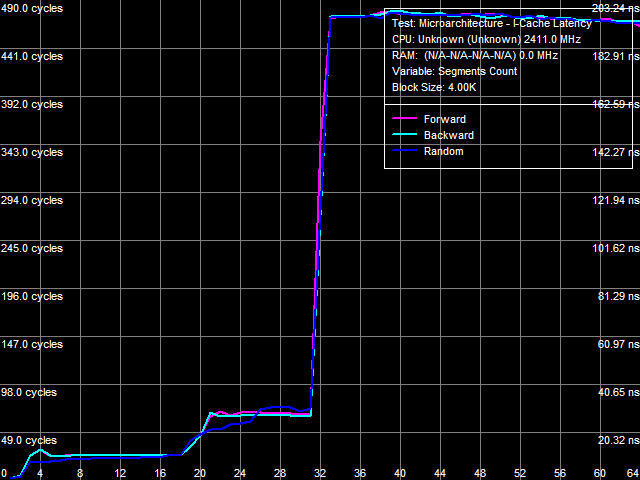 Picture 3. Data Cache Associativity TLB CharacteristicsThe strongest effect from the patch is expectedly demonstrated in TLB tests. TLB characteristics themselves do not change, of course (because these architectural elements belong to the processor core), but the size/associativity miss penalty of the last TLB level grows significantly. 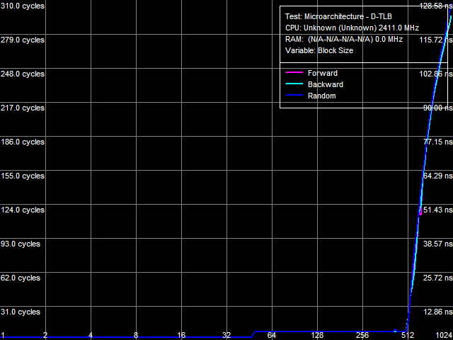 Picture 4. D-TLB size 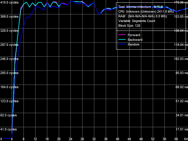 Picture 5. L2 D-TLB Associativity Picture 4 shows results of the D-TLB Size test, and Picture 5 - results of the L2 D-TLB Associativity test. The L2 D-TLB miss penalty grows much in both cases - approximately 290 cycles for size and 400 cycles for associativity. 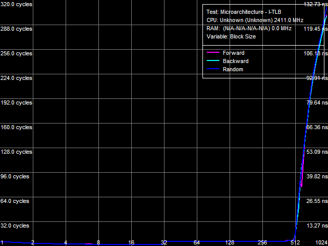 Picture 6. I-TLB size 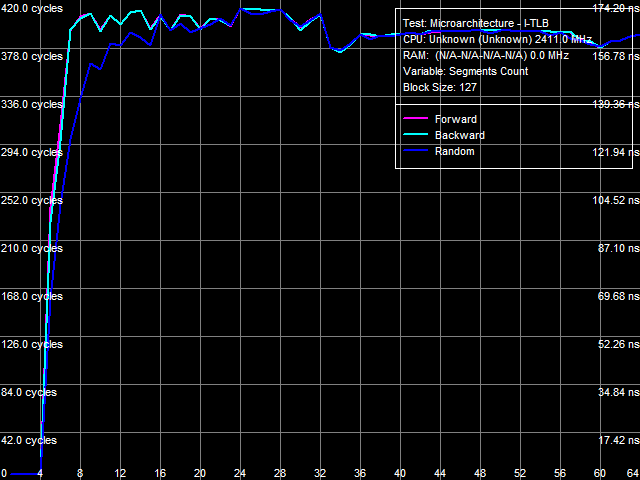 Picture 7. L2 I-TLB Associativity The same results are demonstrated by the I-TLB size (Picture 6) and associativity (Picture 7) tests. The L2 I-TLB miss penalty for size is approximately 300 cycles, and its associativity miss penalty amounts to about 400 cycles, which is close to corresponding values obtained in the D-TLB tests. ConclusionsWhat conclusions follow from our analysis? First of all, we can draw an important conclusion that AMD Phenom (K10) and AMD Athlon 64 (K8) processors indeed contain some structure in their integrated memory controllers, which can be called a large TLB. It's efficient both for data calls (D-TLB) and for code execution (I-TLB). Existence of this structure in both processor families can be proved by moderate miss penalties of the last level (L2) of D-TLB and I-TLB, about 20-40 cycles. When it's disabled (it's the most reasonable explanation of what the patch does with AMD Phenom processors), the above mentioned miss penalties grow significantly (up to 300-400 cycles, that is practically by ten times!) We should also mention Energy Efficient AMD Athlon 64 X2 EE processors here, where miss penalties of L2 D-TLB and I-TLB are initially high. We can assume that such processors either lack the TLB structure in the integrated memory controller (which is unlikely, because we cannot say that it's so hard to implement and consumes so much power, that it had to be removed from Energy Efficient modifications of these processors), or... it's initially disabled because of a bug, similar to the bug in the integrated memory controller in Phenom processors (which is much more likely). The next conclusion, which can be drawn from our test results, is that the above-mentioned TLB structure belongs to the integrated memory controller, not to its L3 Cache (as was mentioned in early reports about the bug in Phenom processors). It's proved by the fact that the patch has practically no negative effect on performance characteristics (bandwidth and latency) of L3 Cache. Thus, a general performance drop in the patched system can be explained solely by the reduced memory performance characteristics, and particularly, by a significantly increased random access latency. Here is a summary table.
It's a bad idea to publish a mean value of the patch effect on so different low-level characteristics - the spread of results varies from 1.7% to 11.8 times. And the effects themselves (for example, the increased TLB miss penalties) are not as strong in real applications, because these characteristics are purely synthetic. However, we can group reduced memory performance characteristics (18-20%), which are close to reality. This reduction is comparable to the reduction of system performance in most real applications, which operate data in a stream rather than in random way. What concerns random data access, we can expect higher performance drops, because the memory access latency in this mode grows significantly. Dmitri Besedin (dmitri_b@ixbt.com)
February 28, 2008 Write a comment below. No registration needed!
|
Platform · Video · Multimedia · Mobile · Other || About us & Privacy policy · Twitter · Facebook Copyright © Byrds Research & Publishing, Ltd., 1997–2011. All rights reserved. | |||||||||||||||||||||||||||||||||||||||||||||||||||||||||||||||||||||||||||||||||||||||||||||||||||||||||||||||||||||||||||||||||||||||||||||||||||||||||||||||||||||||||||||||||||||||||||||||||||||||||||||||||||


