NVIDIA NV4X and G7X Reference
|
NV4X Chip Specifications
| Code name |
|
|
|
|
|
|
|
| Baseline Article |
|
|
|
| Process Technology (nm) |
130 |
110 |
130 |
110 |
| Transistors (M) |
222 |
190 |
143 |
77 |
| Pixel Processors |
16 |
12 |
4 |
2 |
| Texture Units |
16 |
12 |
8 |
4 |
| Blending Units |
16 |
12 |
4 |
2 |
| Vertex Processors |
6 |
3 |
| Memory Bus |
256 (64x4) |
128 (64x2) |
64 (32x2) |
| Memory Types |
DDR, GDDR2, GDDR3
|
| System Bus |
PEG 16x |
AGP 8x |
PEG 16x |
AGP 8x |
PEG 16x |
| RAMDAC |
2 x 400 MHz |
| Interfaces |
TV-Out
TV-In (a video capture chip is required)
2 x DVI (external interface chips are required) |
| Vertex Shaders |
3.0 |
| Pixel Shaders |
3.0 |
| Precision of pixel calculations |
FP16
FP32 |
| Precision of vertex calculations |
FP32 |
| Texture component formats |
FP32 (without filtering)
FP16
I8
DXTC*, S3TC
3Dc (emulation) |
| Rendering formats |
FP32 (without blending and MSAA)
FP16 (without MSAA, no blending is available to NV44)
I8 |
| MRT |
available |
| Antialiasing |
2x and 4x RGMS
SS (in hybrid modes) |
| Z generation |
2x without color |
| Stencil buffer |
Double-sided |
| Shadow technologies |
Hardware shadow maps
Geometry shadow optimizations |
G7X Specifications
| Code name |
|
|
|
|
| Baseline Article |
|
|
|
| Process Technology (nm) |
90 |
110 |
| Transistors (M) |
279 |
178 |
112 |
302 |
| Pixel Processors |
24 |
12 |
4 |
24 |
| Texture Units |
24 |
12 |
4 |
24 |
| Blending Units |
16 |
8 |
2 |
16 |
| Vertex Processors |
8 |
5 |
3 |
8 |
| Memory Bus |
256 (64x4) |
128 (64x2) |
64 (32x2) |
256 (64x4) |
| Memory Types |
DDR, GDDR2, GDDR3 |
| System Bus |
PCI-Express 16x |
| RAMDAC |
2 x 400 MHz |
| Interfaces |
TV-Out
TV-In (a video capture chip is required)
2 x DVI Dual Link (cheaper models offer only one)
HDTV-Out |
| Vertex Shaders |
3.0 |
| Pixel Shaders |
3.0 |
| Precision of pixel calculations |
FP16
FP32 |
| Precision of vertex calculations |
FP32 |
| Texture Formats |
FP32 (without filtering)
FP16
I8
DXTC, S3TC
3Dc (emulation) |
| Rendering formats |
FP32 (without blending and MSAA)
FP16 (without MSAA)
I8 |
| MRT |
available |
| Antialiasing |
TAA (AA of transparent polygons)
2x and 4x RGMS
SS (in hybrid modes) |
| Z generation |
2x without color |
| Stencil buffer |
Double-sided |
| Shadow technologies |
Hardware shadow maps
Geometry shadow optimizations |
Specifications of NV4X and G7X series reference cards
Card |
Chip
Bus |
PS/TMU/VS units |
Core frequency (MHz) |
Memory frequency (MHz) |
Memory capacity (MB) |
Memory bandwidth (GB) |
Texel rate (Mtex) |
Fill
rate (Mpix) |
| GeForce 6800 Ultra |
NV40
AGP |
16/16/6 |
400 |
550(1100) |
256 GDDR3 |
35.2
(256) |
6400 |
| GeForce 6800 |
NV40
AGP |
12/12/6 |
325 |
350(700) |
128
DDR |
22.4
(256)
|
3900 |
| GeForce 6800 GT |
NV40
AGP |
16/16/6 |
350 |
500(1000) |
256
GDDR3 |
32.0
(256)
|
5600 |
| GeForce 6800 LE |
NV40
AGP |
8/8/4 |
320 |
350(700) |
128
DDR |
22.4
(256)
|
2560 |
| GeForce 6600 |
NV43
PEG16x |
4/8/3 |
300 |
350(700) |
128
DDR |
11.2
(128)
|
2400 |
1200 |
| GeForce 6600 GT |
NV43
PEG16x |
4/8/3 |
500 |
500(1000) |
128
GDDR3 |
16.0
(128)
|
4000 |
2000 |
| GeForce 6800 GTO |
NV45
PEG16x |
12/12/5 |
350 |
450(900) |
256 GDDR3 |
28.8
(256) |
4200 |
| GeForce Go 6800 |
NV41M
PEG16x |
12/12/6 |
275 |
300(600) |
256 GDDR3 |
19.2
(256) |
3300 |
| GeForce 6800 |
NV41
PEG16x |
12/12/6 |
325 |
350(700) |
128
DDR |
22.4
(256) |
3900 |
| GeForce 6600 GT |
NV43
AGP |
4/8/3 |
500 |
450(900) |
128
GDDR3 |
14.4
(128) |
4000 |
2000 |
| GeForce 6800 GT |
NV45
PEG16x |
16/16/6 |
350 |
500(1000) |
256
GDDR3 |
32.0
(256) |
5600 |
| GeForce 6800 Ultra |
NV45
PEG16x |
16/16/6 |
400 |
550(1100) |
256 GDDR3 |
35.2
(256) |
6400 |
| GeForce 6200 32TC |
NV44
PEG16x |
2/4/3 |
350 |
350(700) |
32
GDDR |
2.8
(32)
|
1400 |
700 |
| GeForce 6200 64TC |
NV44
PEG16x |
2/4/3 |
350 |
350(700) |
64
GDDR |
5.6
(64) |
1400 |
700 |
| GeForce Go 6200 |
NV44
PEG16x |
2/4/3 |
300 |
300(600) |
16
GDDR |
2.4
(32) |
1200 |
600 |
| GeForce 6800 LE |
NV41
PEG16x |
8/8/4 |
325 |
350(700) |
128
DDR |
19.2
(256) |
2600 |
| GeForce 6600 |
NV43
AGP |
4/8/3 |
300 |
275(550) |
128
DDR |
8.8
(128) |
2400 |
1200 |
| GeForce 6600 LE |
NV43
AGP |
4/4/3 |
300 |
250(500) |
128
DDR |
8.0
(128) |
1200 |
| GeForce 6200 |
NV43
PEG16x |
4/4/3 |
300 |
275(550) |
128
DDR |
4.4
(64) |
1200 |
| GeForce Go 6600 |
NV43
PEG16x |
4/8/3 |
375 |
350(700) |
128
DDR |
11.2
(128) |
3000 |
1500 |
| GeForce Go 6800 Ultra |
NV42
PEG16x |
12/12/5 |
450 |
530(1060) |
256 GDDR3 |
33.9
(256) |
5400 |
| GeForce 6800 Ultra |
NV45
PEG16x |
16/16/6 |
400 |
525(1050) |
512 GDDR3 |
33.6
(256) |
6400 |
| GeForce 6200 A |
NV44A
AGP |
2/4/3 |
350 |
250(500) |
128
GDDR |
4.0
(64) |
1400 |
700 |
| GeForce Go 6800 |
NV42
PEG16x |
12/12/5 |
450 |
550(1100) |
128 GDDR3 |
35.2
(256) |
5400 |
| GeForce 7800 GTX |
G70
PEG16x |
24/24/8 |
430 |
600(1200) |
256 GDDR3 |
38.4
(256) |
10320 |
6880 |
| GeForce 7800 GTX 512Mb |
G70
PEG16x |
24/24/8 |
550 |
850(1700) |
512 GDDR3 |
54.4
(256) |
13200 |
8800 |
| GeForce 7800 GT |
G70
PEG16x |
20/20/7 |
400 |
500(1000) |
256 GDDR3 |
32.0
(256) |
8000 |
6400 |
| GeForce 7800 GS |
G70
AGP |
16/16/6 |
375 |
600(1200) |
256 GDDR3 |
38.4
(256) |
6000 |
6000 |
| GeForce 7300 LE |
G72
PEG16x |
4/4/3 |
450 |
300(600) |
128 GDDR2 |
4.8
(64) |
1800 |
900 |
| GeForce 7300 GS |
G72
PEG16x |
4/4/3 |
550 |
350(700) |
256 GDDR2/GDDR3 |
5.6
(64) |
2200 |
1100 |
| GeForce 7300 GT |
G73
PEG16x |
8/8/4 |
350 |
333(667) |
128-256 GDDR3 |
10.7
(128) |
2800 |
1400 |
| GeForce 7600 GS |
G73
PEG16x |
12/12/5 |
400 |
400(800) |
256 GDDR2 |
12.8
(128) |
4800 |
3200 |
| GeForce 7600 GT |
G73
PEG16x |
12/12/5 |
560 |
700(1400) |
256 GDDR3 |
22.4
(128) |
6720 |
4480 |
| GeForce 7900 GTX |
G71
PEG16x |
24/24/8 |
650 |
800(1600) |
512 GDDR3 |
51.2
(256) |
15600 |
10400 |
| GeForce 7900 GT |
G71
PEG16x |
24/24/8 |
450 |
660(1320) |
256 GDDR3 |
42.2
(256) |
10800 |
7200 |
| GeForce 7950 GX2 |
2xG71
PEG16x |
2x(24/24/8) |
500 |
600(1200) |
2x512 GDDR3 |
2x38.4
(2x256) |
2x12000 |
2x8000 |
card |
chip
bus |
PS/TMU/VS units |
Core frequency (MHz) |
Memory frequency (MHz) |
Memory capacity (MB) |
Memory bandwidth (GB) |
Texel rate (Mtex) |
Fill
rate (Mpix) |
The main theoretical, practical, and comparative materials
Theoretical materials and reviews of video cards, which concern functional properties of the GPU ATI R4XX/R5XX and NVIDIA NV4X/G7X
- NVIDIA GeForce 6800GT (NV40). Part 1 — Architectural Peculiarities and Synthetic Tests in D3D RightMark
- NVIDIA GeForce 6800GT (NV40). Part 2 - Analysis of Performance and Quality in Game Applications
- ATI RADEON X800 XT and X800 PRO (R420)
- The Battle of Borodino Between ATI RADEON X800 XT and NVIDIA GeForce 6800GT. Episode Two: 450 MHz in the Latter and New Tests of Both Cards
- The Battle of Borodino Between ATI RADEON X800 and NVIDIA GeForce 6800: Episode Three - Trilinear Filtering (Synthetic Examples)
- The Battle of Borodino Between ATI RADEON X800 and NVIDIA GeForce 6800: Episode Four: Filtering Tests in RightMark
- The Battle of Borodino Between ATI RADEON X800 and NVIDIA GeForce 6800 - Episode Five: Filtering Tests in Games
- PowerColor RADEON X800 PRO Limited Edition, hardware reconstruction of X800 PRO into X800 XT Platinum Edition
- HIS Excalibur 9550, HIS Excalibur X800 PRO, as well as a Comparison of RADEON X800 PRO and GeForce 6800GT and Scalability
- NVIDIA GeForce 6800 GT
- The Battle of Borodino Between ATI RADEON X800 and NVIDIA GeForce 6800 - Episode Six: Filtering in Games (Continuation)
- NVIDIA GeForce 6800 GT PCI-E (NV45)
- Brief Account of FarCry v.1.2 Tests and of the First Shader 3.0 Implementation
- ABIT RADEON X800 PRO, X600XT based on ATI X800PRO/X600XT
- Leadtek WinFast A400 GT TDH based on NVIDIA GeForce 6800 GT
- Gigabyte GV-RX80X256V RADEON X800 XT Platinum Edition
- FarCry v.1.2 Tests Continued and Shader 2.0b
- HIS Excalibur X800 Pro/X800 XT IceQ II Limited Edition Based on ATI X800PRO/X800XT
- MSI NX6800-TD128, Galaxy Glacier GeForce 6800 Based on NVIDIA GeForce 6800
- ASUS AX 800 PRO/AX 800 XT based on ATI X800PRO/X800XT
- Chaintech Apogee NVIDIA GeForce 6800GT Based on NVIDIA GeForce 6800GT — Tests in DOOM III with "Optimizations"
- Sapphire RADEON X800 XT
- Palit GeForce 6800 and GeForce PCX5750
- Sapphire Atlantis RADEON X800 XT AGP/PCI-E Based on ATI RADEON X800 XT
- ASUS V9999 Ultra Deluxe Based on NVIDIA GeForce 6800 Ultra
- Gigabyte GV-N68U256D Based on GeForce 6800 Ultra
- NVIDIA GeForce 6600GT and 6600 (NV43): Part 1 — Performance
- ATI RADEON X700XT (RV410): Part 1 — Performance
- Galaxy Glacier GeForce 6800GT Based on NVIDIA GeForce 6800GT
- Leadtek WinFast PX6600 TD Based on NVIDIA GeForce 6600
- Sapphire Hybrid RADEON X700 PRO 256MB Based on ATI RADEON X700 PRO
- HIS Excalibur RADEON X800XT Limited Edition PCI-E
- ATI RADEON X800SE 256MB AGP
- Gainward PowerPack Ultra/2400 Golden Sample Based on NVIDIA GeForce 6800GT
- Testing NVIDIA SLI (GeForce 6800/6600 PCI-E). Part 1 — iE7525 Platform
- Testing NVIDIA SLI (GeForce 6800/6600 PCI-E). Part 2 - NVIDIA nForce4 SLI Platform
- ATI RADEON X850XT PE 256MB PCI-E
- Video cards from Albatron, Gainward, Gigabyte, Innovision, Leadtek and Palit based on NVIDIA GeForce 6200/6600/6600GT
- ASUS V9999GT 128MB DDR Based on NVIDIA GeForce 6800GT
- Leadtek WinFast PX6600GT AGP 128MB
- NVIDIA GeForce 6200 TurboCache PCI-E
- ASUS V9999 Ultra/TD, ASUS AX800XT Platinum Based on NVIDIA GeForce 6800 Ultra, ATI RADEON X800XT PE
- Video cards from ASUSTeK, Axle, Gigabyte, Galaxy, Leadtek, Prolink and Palit based on NVIDIA GeForce 6200/6600/6600GT
- Video cards from Sapphire Based on ATI RADEON X700PRO/X800/X800XL/X850XT
- MSI GeForce 6800 PCI-E (NX6800) 256MB (NV41)
- TUL Video Cards Based on ATI RADEON X800/X800XL/X850XT
- Gigabyte 3D1 (2xGeForce 6600GT) and K8NXP-SLI Motherboard
- ASUS Extreme N6800 Based on GeForce 6800 (SLI) and A8N-SLI-Deluxe Motherboard
- Leadtek Video Cards Based on NVIDIA GeForce 6200TC/6600/6800Ultra as well as GeForce 6800 Ultra SLI
- GeForce 6800 Ultra PCI-E, 6800GT PCI-E, 6600GT AGP, RADEON X850XT PE, X800 XL from ASUSTeK
- Albatron Video Cards Based on NVIDIA GeForce 6200/6600/6600GT
- ATI RADEON X850 XT AGP 256MB Represented by HIS RADEON X850 XT AGP IceQ II Turbo 256MB; HIS RADEON X850 XT Platinum AGP IceQ II 256MB
- ATI RADEON X850 PRO PCI-E 256MB; ATI RADEON X300SE HyperMemory 32 (128)MB PCI-E; ATI RADEON X800 AGP 256MB Represented by Sapphire Video Cards as well as Sapphire RADEON X850XT PE AGP 256MB and Sapphire RADEON X800XL Ultimate PCI-E 256MB
- MSI RX800 XL-VT2D256E PCI-E Based on ATI RADEON X800 XL
- Inno3D GeForce 6200A 128MB AGP Based on NVIDIA GeForce 6200A (NV44A)
- NVIDIA GeForce 7800 GTX 256MB PCI-E: Part 1 - Theory and Architecture
- NVIDIA GeForce 7800 GTX 256MB PCI-E: Part 2: Video card's features, synthetic tests
- NVIDIA GeForce 7800 GTX 256MB PCI-E: Part 3: Game tests, AA quality, conclusions
- NVIDIA GeForce 7800 GTX 256MB PCI-E. Part 4: Transparent antialiasing
- Gigabyte 3D1-68GT (Dual GeForce 6800GT) 2x256MB PCI-E
- Albatron GeForce 6800 128MB PCI-E (PC6800) Based on NVIDIA GeForce 6800 (NV42)
- Palit GeForce 7800 GT 256MB Based on NVIDIA GeForce 7800 GT (G70)
- ASUS Extreme N7800 GTX 256MB, ASUS Extreme N7800 GTX TOP 256MB Based on NVIDIA GeForce 7800 GTX
- Leadtek WinFast PX7800GT TDH myVIVO Extreme 256MB, Leadtek WinFast Duo PX6600GT TDH Extreme 256MB Based on NVIDIA GeForce 7800 GT, 6600 GT
- Gigabyte GeForce 7800GTX TurboForce 256MB, Gigabyte RADEON X800 XL 512MB Based on NVIDIA GeForce 7800 GTX, ATI RADEON X800 XL
- ATI RADEON X1800 (R520), X1600 (RV530) and X1300 (RV515): Part 1. Theory and architecture
- ATI RADEON X1800 (R520), X1600 (RV530) and X1300 (RV515). Part 2: Video cards' features, synthetic tests
- ATI RADEON X1800 (R520), X1600 (RV530) and X1300 (RV515): Part 3: Performance in Game Tests
- ATI RADEON X1800 (R520), X1600 (RV530) and X1300 (RV515): Part 4: Rendering Quality, New Anti-Aliasing and Anisotropic Filtering Modes
- ATI RADEON X1800 (R520), X1600 (RV530) and X1300 (RV515): Part 5: Brief Introduction into AVIVO and Bottom Line
- ATI RADEON X1800 (R520), X1600 (RV530) and X1300 (RV515): Part 6: Interview with Guennadi Riguer (ATI Technologies)
- NVIDIA GeForce 6800 GS 256MB, NVIDIA GeForce 6600 DDR2 256MB
- HIS RADEON X1800 XL 256MB PCI-E Based on ATI RADEON X1800 XL
- NVIDIA GeForce 7800 GTX 512MB
- HIS RADEON X1800 XT 512MB PCI-E Based on ATI RADEON X1800 XT
- ASUS Extreme Dual N7800GT 512MB
- Gainward GF7800GTX 512MB GS, 7800GT GS, PSU Hiper Type-R HPU-4R580
- Video Cards from Sapphire Based on ATI RADEON X800GT/X800GTO/X800GTO2/X1300/X1600XT/X1800XL/X1800XT
- ATI Technologies' Counter-Offensive is Still in Progress: RADEON X1900 XTX/XT (R580): Part 1. Theory and architecture
- ATI Technologies' Counter-Offensive is Still in Progress: RADEON X1900 XTX/XT (R580): Part 2: Video card's features, synthetic tests
- ATI Technologies' Counter-Offensive is Still in Progress: RADEON X1900 XTX/XT (R580): Part 3: Performance in Game Tests
- ATI CrossFire Based on RADEON X1900 XT, 2x512MB
- Video cards from ASUSTeK Based on ATI RADEON X700/X800/X1800XL/X1800XT NVIDIA GeForce 7800GT
- Gainward Bliss 7800GT/6800GS Goes Like Hell 512MB PCI-E Based on NVIDIA GeForce 7800 GT/6800 GS
- HIS IceQ II RADEON X1600 XT iTurbo 256MB PCI-E Based on RADEON X1600 XT
- HIS IceQ RADEON X1600 PRO Turbo 128MB PCI-E Testing X1600 PRO Turbo 2x128MB CrossFire
- New-old RADEON X1800: Now GTO — a Very Powerful Competitor to GeForce 7600 GT
- Thinness rules! 0.09 Calibre, a Volley from California: NVIDIA GeForce 7900 GTX/GT (G71), GeForce 7600 GT (G73) — Part 1: Theory and architecture
- Thinness rules! 0.09 Calibre, a Volley from California: NVIDIA GeForce 7900 GTX/GT (G71), GeForce 7600 GT (G73) — Part 2: Video cards' features, synthetic tests
- Thinness rules! 0.09 Calibre, a Volley from California: NVIDIA GeForce 7900 GTX/GT (G71), GeForce 7600 GT (G73) — Part 3: Performance in Game Tests
- Thinness rules! 0.09 Calibre, a Volley from California: NVIDIA GeForce 7900 GTX/GT (G71), GeForce 7600 GT (G73). Part 4: NVIDIA Editor's Day 28.02.2006
- Thinness rules! 0.09 Calibre, a Volley from California: NVIDIA GeForce 7900 GTX/GT (G71), GeForce 7600 GT (G73). Part 5: HD Video Support
- Last of the Mohicans: Four New AGP Cards — RADEON X1300/X1600 PRO, GeForce 7800 GS from GeCube, Sapphire, and Leadtek. A finale in the AGP epoch.
- NVIDIA GeForce 7600 GS - a middle-end product for $120-$140 easily outperforming its competitor
- Three budget accelerators based on the new GeForce 7300 GS from Albatron, MSI, and Palit that demonstrate good results for their price
- A new product from ATI in the $300 price segment - RADEON X1900 GT: a card from Sapphire
- BFG GeForce 7950 GX2 1GB PCI-E - the most powerful stand-alone accelerator these days, though with two GPUs
- Three accelerators from ASUSTeK: GeForce 7900GTX / 7950GX2 / 7600GT — all of them copy the reference design, only 7600 GT has a unique cooling system
Details: NV40/NV45, GeForce 6800 Family
NV40/NV45 Specifications
- Code name: NV40/NV45
- Process technology: 130nm FSG (IBM)
- 222 million transistors
- FC package (flip-chip, flipped chip without a metal cap)
- 256 bit memory interface
- Up to 1 GB of DDR/DDR2/GDDR3 memory
- AGP 3.0 8x bus interface in the NV40, PCI Express 16x in the NV45 (the second chip is integrated into the package — HSI bridge)
- Special APG 16x mode (in both directions) for PCI Express of the HSI bridge
- 16 pixel processors, each with a texture unit with random floating point and integer filtering (anisotropy up to 16x).
- 6 vertex processors, each of them has a texture unit without sample filtering (discrete sampling)
- Calculating, blending, and writing up to 16 full (color, depth, stencil buffer) pixels per clock
- Calculating and writing up to 32 values of Z buffer and stencil buffer per clock (if no color operations are performed)
- Support for two-sided stencil buffer
- Support for special geometry render optimizations to accelerate shadow algorithms based on stencil buffer (so called Ultra Shadow II technology)
- Everything necessary to support pixel and vertex Shaders 3.0, including dynamic branching in pixel and vertex processors, vertex texture fetch, etc.
- Texture filtering in floating point format
- Support for a frame buffer in floating point format (including blending operations)
- MRT (Multiple Render Targets — rendering into several buffers)
- 2x RAMDAC 400 MHz
- 2x DVI interfaces (external chips are required)
- TV-Out and TV-In (require interface chips)
- Programmable streaming video processor (for encoding, decoding, and video post processing purposes)
- 2D accelerator supporting all GDI+ functions
GeForce 6800 Ultra AGP Reference Card Specifications
- Core clock: 400 MHz
- Effective memory frequency: 1.1 GHz (2*550 MHz)
- Memory type: GDDR3
- Memory: 256 MB
- Memory bandwidth: 35.2 GB/sec.
- Maximum theoretical fillrate: 6.4 gigapixel per second.
- Theoretical texture sampling rate: 6.4 gigatexel per second.
- 2 x DVI-I connectors
- TV-Out
- Consumes up to 120 W (the card is equipped with two additional power connectors, recommended PSUs start from 480 W)
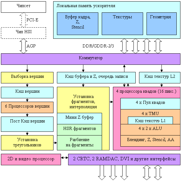
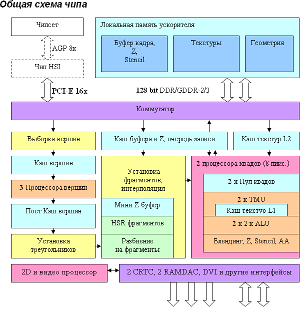
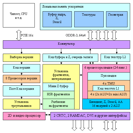
Chip Architecture
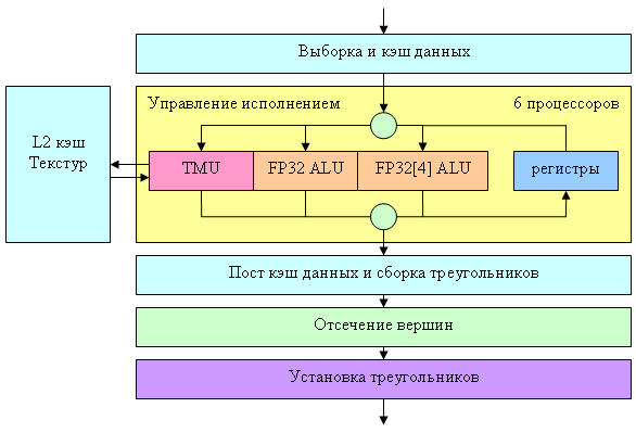
Here is a flow chart of the NV40 vertex processor:
The processor itself is indicated by a yellow rectangle, the other units are shown to make the picture complete. NV40 is declared to have 6 independent processors (visualize the yellow unit copied six times), each one executing its own instructions and having its own flow control (that is different processors can execute different conditional branches over different vertices simultaneously). A vertex processor of the NV40 can execute the following operations per clock: one vector operation (up to four FP32 components), one scalar FP32 operation, and one access to a texture. It supports integer and floating point texture formats and mip-mapping. One vertex shader may use up to four different textures. But there is no filtering – only the simplest discrete access to the nearest value by specified coordinates. Here is a summary table with the NV40 vertex processor parameters from the point of view of DX9 vertex shaders compared to R3XX and NV3X families:
| Vertex Shader Model |
2.0 (R 3 XX)
|
2. a (NV 3 X)
|
3.0 (NV40)
|
| Instructions in shader code |
256
|
256
|
over 512
|
| The number of executed instructions
|
65535
|
65535
|
over 65535
|
| Predicates |
Not available
|
Available
|
Available
|
| Temporal Registers |
12
|
13
|
32
|
| Constant Registers |
over 256
|
over 256
|
over 256
|
| Static Branching |
Available
|
Available
|
Available
|
| Dynamic Branching |
Not available
|
Available
|
Available
|
| Nesting depth of dynamic branching
|
Not available
|
24
|
24
|
| Texture Sampling |
Not available
|
Not available
|
Available (4)
|
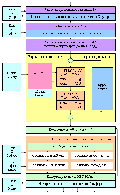
Let's analyze the pixel architecture of the NV40 in the order of the data flow.
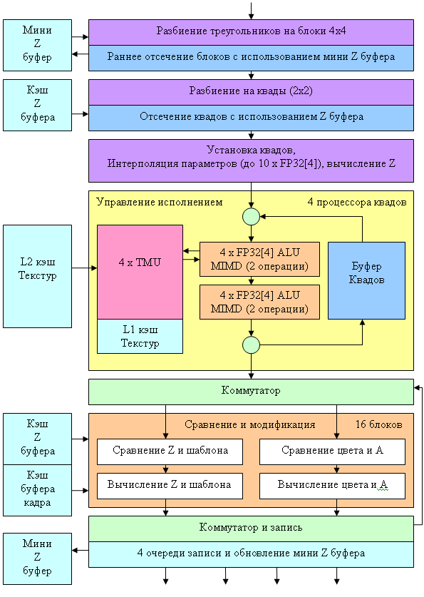
We shall dwell on the most interesting facts. Firstly, while the NV3X had only one quad processor, processing a block of four pixels (2x2) per clock, there are four such processors now. They are completely independent, each of them can be excluded from operation (for example, to create a light version of a chip with three processors, if one of them is not effective). There is still a queue for the quad "carrousel" in each processor (see DX Current), its own queue in each processor. Consequently, there remains a similar approach to pixel shader execution (like in NV3X): running more than a hundred quads through one setting (operation) and subsequent change of the setting in accordance with the shader code. But there are noticeable differences as well. The number of TMUs in the first place – now we have only one TMU for each quad pixel. There are 4 quad processors all in all, each having 4 TMUs, 16 in total. The new TMUs support 16:1 anisotropic filtering (so called 16x, NV3X offered only 8x) and they have finally learnt to apply all kinds of filtering with floating point texture formats. But that's only in case of 16 bit component precision (FP16). Filtering is still unavailable for FP32, but even FP16 is a noticeable progress – now floating point textures will be full alternative to integer textures in any applications. Especially as FP16 texture filtering comes with no performance loss (however, the increased data flow may and must have an effect on performance of real applications). Note the bi-level organization of texture caching – each quad processor has its own L1 Texture Cache. Its necessity is conditioned by two facts – (1) fourfold increase in the number of simultaneously processed quads (the quad queue in a processor did not grow longer, but there are four processors now) and (2) competitive access from vertex processors to the texture cache. There are two ALUs for each pixel, each of them can perform two different (!) operations over a diverse number of arbitrary selected vector components (up to 4x). That is the available schemes include 4, 1+1, 2+1, 3+1 (like in the R3XX) and the new 2+2 configuration, previously unavailable. For more details read DX Current. Arbitrary masking and post-operational component rearrangement are supported. Besides, ALU can normalize a vector as a single operation, which may have a significant effect on performance of some algorithms. Hardware SIN and COS calculations were removed from the new NVIDIA architecture. Practice showed that transistors used for this feature had been just wasted – access by the simplest grid (1D texture) provides better results in terms of performance, especially considering that ATI does not offer this support. Thus, depending on code, from one to four different FP32 operations can be performed over vectors and scalars per clock. You can see on the diagram that the first ALU is used for overhead operations during texture sampling. Thus, a single clock can be spent either to get one texture sample and use the second ALU for one or two operations, or to use both ALUs, if we don't get a texture sample during this pass. Performance of this tandem directly depends on a compiler and code. But we obviously have Minimum: one texture sample per clock
Minimum: two operations per clock without texture sampling
Maximum: four operations per clock without texture sampling
Maximum: one texture sample and two operations per clock We have information that the number of temporal registers for each quad was doubled, that is now we have 4 temporal FP32 registers per pixel or 8 temporal FP16 registers. This fact must boost the performance of complex shaders. Besides, any hardware limitations on the length of pixel shaders and the number of texture samples are lifted – it's now up to API only. The most important improvement is the dynamic flow control. Here is a summary table of features:
|
Pixel Shader Model
|
2.0 (R3XX)
|
2.a (NV3X)
|
2.b (R420)
|
3.0 (NV40)
|
|
Texture sampling nesting up to
|
4
|
Not limited
|
4
|
Not limited
|
|
Texture sampling up to
|
32
|
Not limited
|
Not limited
|
Not limited
|
|
Shader code length
|
32 + 64
|
512
|
512
|
over 512
|
|
Shader instructions
|
32 + 64
|
512
|
512
|
over 65535
|
|
Interpolators
|
2 + 8
|
2 + 8
|
2 + 8
|
10
|
|
Predicates
|
not available
|
available
|
not available
|
available
|
|
Temporal Registers
|
12
|
22
|
32
|
32
|
|
Constant Registers
|
32
|
32
|
32
|
224
|
|
Arbitrary component rearrangement
|
not available
|
available
|
not available
|
available
|
|
Gradient instructions (D D X/ D DY)
|
not available
|
available
|
not available
|
available
|
|
Nesting depth of dynamic branching
|
not available
|
not available
|
not available
|
24
|
And now let's get back to our scheme and pay attention to its bottom part. You can see a unit there that is responsible for comparing and modifying color, transparency, Z and stencil values. We have the total of 16 such units. As the comparison and modification task is rather homogeneous, we can use this unit in two modes:
Standard mode (the following operations are completed per clock):
- Comparison and modification of a Z-value
- Comparison and modification of a stencil-value
- Comparison and modification of the transparency and color component (blending)
Turbo mode (the following operations are completed per clock):
- Comparison and modification of two Z values
- Comparison and modification of two stencil values
It goes without saying that the latter mode is possible only when there is no calculated color value being written. That's why the specifications run that in case of no color, the chip can fill 32 pixels per clock. Besides, it will calculate both the Z value as well as the stencil value. In the first place, such a turbo mode will come in handy to accelerate rendering shadows based on the stencil buffer (like in Doom III) and for a rendering pre-pass, which calculates only Z buffer (this technique often allows to save time on long shaders, as the overlay factor will certainly go down to 1).
They finally repaired the annoying omission of the MRT support (Multiple Render Targets – rendering into several buffers) in the NV3X family – that is one pixel shader can calculate and write up to four different color values to be put into different buffers (of the same size). The lack of this feature in the NV3X made up a serious case for the R3XX for developers. Now this feature appeared in the NV40. Another important difference from previous generations is the intensive support for floating point arithmetic in this unit. All operations (comparing, blending, writing colors) may be performed in FP16 component format. Finally we get the so called full (orthogonal) support for 16bit floating point operations, in terms of filtering and texture sampling as well as frame buffer operations. The next in turn is FP32, but it's probably up to the next generation.
There is another interesting fact – MSAA support. Like its predecessors (NV 2X and NV 3 X), NV40 is capable of 2 x MSAA without performance losses (two Z values for one pixel are generated and compared). In case of 4 x MSAA, one penalty clock should be added (in practice, there is no need to calculate all the four values per clock – it will be hard to write all these values into Z and frame buffers per clock – the memory bandwidth is limited). MSAA higher than 4x is not supported – like in the previous family, all more complex modes are hybrids between 4x MSAA and subsequent SSAA of this or that size. But now RGMS is finally supported (MSAA Rotated Grid Sample):
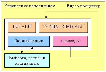
This separate programmable unit in NV40 is responsible for processing video streams:
This processor contains four functional units (INT ALU, INT SIMD ALU with 16 components, load/write data unit, and branch unit) and thus can execute up to four different operations per clock. Data format – integer numbers, probably 16 bit or 32 bit precision (we don't know for sure, but 8 bit wouldn't be enough for some algorithms). The processor includes special sampling, dispatch, and writing data steams functions. Classic decoding and encoding video tasks (IDCT, deinterlacing, color model converting, etc) can be performed without loading CPU. But CPU management is still required – data preparation and selection of conversion parameters are still performed by CPU, especially in case of complex compression algorithms including decompression as one of intermediate steps. This processor can significantly unload CPU, especially in case of high video resolutions, like HDTV formats, which are getting increasingly popular. We don't know whether these processor capacities are used for 2D acceleration, especially some complex GDI+ functions — it would be logical to use it here. But we don't have information on this aspect yet. Anyway, NV40 complies with the highest requirements to 2D hardware acceleration – all necessary calculation-intensive GDI and GDI+ functions are executed on the hardware level.
Details: NV43, GeForce 6600[GT]
NV43 Specifications
- Code name: NV43
- Process technology: 110nm (TSMC)
- 146 million transistors
- FC package (flip-chip, flipped chip without a metal cap)
- 128 bit memory interface
- Up to 256 MB of DDR/DDR2/GDDR3 memory
- On-chip PCI-Express 16x bus interface
- Interface translation into APG 8x via the bidirectional PCI Express<->AGP HSI bridge
- 8 pixel processors, each with a texture unit with random floating point and integer filtering (anisotropy up to 16x).
- 3 vertex processors, each with a texture unit, without filtering samples (discrete sampling)
- Calculating, blending, and writing up to 4 full (color, depth, stencil buffer) pixels per clock
- Calculating and writing up to 8 values of Z buffer and stencil buffer per clock (if no color operations are performed)
- Support for two-sided stencil buffer
- Support for special geometry rendering optimizations to accelerate shadow algorithms based on a stencil buffer (so called Ultra Shadow II Technology), particularly widely used in the Doom III engine
- Everything necessary to support pixel and vertex Shaders 3.0, including dynamic branching in pixel and vertex processors, vertex texture fetch, etc.
- Texture filtering in floating point format
- Support for a frame buffer in floating point format (including blending operations)
- MRT (Multiple Render Targets — rendering into several buffers)
- 2 x RAMDAC 400 MHz
- 2 x DVI (external interface chips are required)
- TV-Out and TV-In (interface chips are required)
- Programmable streaming video processor (for encoding, decoding, and video post processing purposes)
- 2D accelerator supporting all GDI+ functions
Reference card GeForce 6600 GT specifications
- Core clock: 500 MHz
- Effective memory frequency: 1 GHz (2*500 MHz)
- 128-bit memory bus
- Memory type: GDDR3
- Memory: 128 MB
- Memory bandwidth: 16 GB/sec.
- Theoretical fill rate: 2 gigapixel/sec.
- Theoretical texture sampling rate: 4 gigatexel per second.
- 1 x VGA (D-Sub) and 1 x DVI-I
- TV-Out
- Consumes up to 70 W (that is there is no need in an additional power connector on PCI-Express cards, the recommended power supply unit is 300 W or more)
NV43 Architecture
There are no special architectural differences from NV40, which is not surprising - NV43 is a scaled down (by means of reducing vertex and pixel processors and memory controller channels) solution based on the NV40 architecture. The differences are quantitative (bold elements on the diagram) but not qualitative - the chip remains practically unchanged from the architectural point of view.
Thus, we have three (instead of six) vertex processors and two (instead of four) independent pixel processors, each working with one quad (2x2 pixel fragment). Interestingly, this time PCI-Express support has become native (that is integrated into a chip), while AGP 8x cards will have to use an additional bidirectional PCI-Ex <-> AGP bridge (shown with a dotted line), which has been already described. Besides, note an important limiting factor - a two-channel controller and a 128-bit memory bus - this fact was analyzed in our review.
The architecture of vertex and pixel processors remained the same - these elements were described in detail above in the NV40/NV45 section. Vertex and pixel processors in NV43 remained the same, but the internal caches could be reduced proportionally to the number of pipelines. However, the number of transistors does not give cause for trouble. Considering not so large cache sizes, it would be more reasonable to leave them as they were in NV40, thus compensating for the noticeable scarcity of the memory pass band. A large ALU array, which contains a lot of transistors, responsible for post processing, verification, Z generation, and pixel blending to write the results to frame buffer, was also reduced in each pipeline compared to NV40. The reduced memory band will not allow to write 4 full gigapixels per second anyway, and the fill rate potential (8 pipelines for 500 MHz) will be used well only with more or less complex shaders with more than two textures and attendant shader calculations.
Details: NV44, GeForce 6200 Family
NV44 Specifications
- Code name: NV44
- Process technology: 110nm (TSMC)
- 77 million transistors
- FC package (flip-chip, flipped chip without a metal cap)
- 64 bit dual channel memory interface
- Up to 64 MB of DDR/DDR2/GDDR3 memory
- On-chip PCI-Express 16x bus interface
- Advanced features of the system memory addressed via PCI Express to store the frame buffer, textures, and other information traditionally stored in local memory
- 4 pixel processors, each with a texture unit with random floating point and integer filtering (anisotropy up to 16x).
- 3 vertex processors, each with a texture unit, without filtering samples (discrete sampling)
- Calculating, blending, and writing up to 2 full (color, depth, stencil buffer) pixels per clock
- Calculating and writing up to 4 values of Z buffer and stencil buffer per clock (if no color operations are performed)
- Support for two-sided stencil buffer
- Support for special geometry rendering optimizations to accelerate shadow algorithms based on a stencil buffer (so called Ultra Shadow II Technology), particularly widely used in the Doom III engine
- Everything necessary to support pixel and vertex Shaders 3.0, including dynamic branching in pixel and vertex processors, vertex texture fetch, etc.
- Texture filtering in floating point format
- Support for a frame buffer in floating point format; FP16 blending is not supported, unlike others chips from this family
- MRT (Multiple Render Targets — rendering into several buffers)
- 2 x RAMDAC 400 MHz
- 2 x DVI (interface chips are required)
- TV-Out and TV-In (interface chips are required)
- Programmable streaming video processor (for encoding, decoding, and video post processing purposes)
- 2D accelerator supporting all GDI+ functions
Reference GeForce 6200 TC-16/TC-32 Specifications
- Core clock: 350 MHz
- Effective memory frequency: 700 MHz (2*350 MHz)
- Memory bus: 32 bit/64 bit
- Memory type: DDR2
- Memory: 16 MB/32 MB
- Memory bandwidth: 2.8 GB per second / 5.6 GB per second
- Theoretical fill rate: 700 megapixel/sec.
- Theoretical texture sampling rate: 1.4 gigatexel per second.
- 1 x VGA (D-Sub) and 1 x DVI-I
- TV-Out
- PCI-Express card does not require an additional power connector
NV44 Architecture
There are no global architectural differences from NV40 and NV43, there are just some innovations in the pixel pipeline aimed at more effective operations with system memory as a frame buffer. On the whole, NV44 is a scaled down (reduced number of vertex and pixel processors and memory controller channels) solution, based on the NV40 architecture. The differences are quantitative (bold elements on the diagram) but not qualitative - the chip remains practically unchanged from the architectural point of view, for the only exception - no FP16 blending.
We have three vertex processors, like in NV43, and one (instead of two) independent pixel processor that operates with one quad (2x2 pixel fragment). PCI Express has become a native on-chip bus interface as in case with the NV43. AGP 8x cards with this chip (TurboCache modification) are not manufactured, as the idea of efficient usage of system memory for rendering requires the adequate bidirectional throughput of the graphics bus.
A very important constraint is a dual-channel memory controller with a 64-bit bus, its limitations are described in detail in our reviews. Judging from the chip package and the number of pins, 64 bit is the hardware limit for the NV44 and 128 bit cards cannot be based on this design, they are based on the NV43 in the 6200 family. The architecture of vertex and pixel processors as well as of the video processor remained the same — these elements have been described in detail above. Except for the declared updates for effective addressing of system memory from texture and blending units. But that's only what is said out loud — we have solid reasons to think that all these features, not so critical and most likely based on Common Cache and Crossbar manager, were included into the NV4X family from the very beginning. There are just no reasons to use them on the level of drivers in senior cards with faster local memory. There is also no point in this technology for AGP cards. Their interface will inevitably become the bottleneck because of the low write speed into the system memory, comparable to PCI. That's how NVIDIA explains the differences in its articles:
… regular architecture and NV44 with TurboCache:
You can obviously see the difference due to data feed for textures and the additional way to write frame data (blending) into the system memory. However, the initial architecture of the chip with a crossbar, treating the graphics bus almost as the fifth channel of the memory controller, may be initially capable of this (starting from the NV40 and even earlier). It's hard to tell whether the NV44 has architectural changes as far as writing and reading data is concerned or these features are just implemented on the driver level.
On the other hand, we shall not deny that it would be optimal to have some paging MMU and dynamic data swapping from system to local memory, which would be treated as L3 Cache. In case of such architecture everything falls to its place. The efficiency will be noticeably higher than discrete allocation of objects and minor hardware revisions will be justified. Especially as having tested this paging unit, one might use it in future architectures, which to all appearances shall be equipped with such units.
Details: G70, GeForce 7800 GTX
G70 Specifications
- Codename: G70 (previously known as NV47)
- Process technology: 110 nm (estimated manufacturer: TSMC)
- 302 million transistors
- FC package (flip-chip, flipped chip without a metal cap)
- 256 bit memory interface
- Up to 1 GB of GDDR3 memory
- PCI Express 16x
- 24 pixel processors, each of them has a texture unit with arbitrary filtering of integer and floating point FP16 textures (including anisotropy, up to 16x inclusive) and "free-of-charge" normalization of FP16 vectors. Pixel processors are improved in comparison with NV4X — more ALUs, effective execution of the MAD operation.
- 8 vertex processors, each of them has a texture unit without sample filtering (discrete sampling).
- Calculating, blending, and writing up to 16 full (color, depth, stencil buffer) pixels per clock
- Calculating and writing up to 32 values of Z buffer and stencil buffer per clock (if no color operations are performed)
- Support for two-sided stencil buffer
- Support for special geometry render optimizations to accelerate shadow algorithms based on stencil buffer and hardware shadow maps (so called Ultra Shadow II technology)
- Everything necessary to support pixel and vertex Shaders 3.0, including dynamic branching in pixel and vertex processors, vertex texture fetch, etc.
- Texture filtering in FP16 format
- Support for a floating point frame buffer (including blending operations in FP16 format and only writing in FP32 format)
- MRT (Multiple Render Targets — rendering into several buffers)
- 2x RAMDAC 400 MHz
- 2 x DVI (external interface chips are required)
- TV-Out and HDTV-Out are built into the chip
- TV-In (an interface chip is required for video capture)
- Programmable hardware streaming video processor (for video compression, decompression, and post processing), a new generation offering performance sufficient for high-quality deinterlacing HDTV
- 2D accelerator supporting all GDI+ functions
- SLI support
Reference card GeForce 7800 GTX specifications
- Core clock: 430 MHz
- Effective memory frequency: 1.2 GHz (2*600 MHz)
- Memory type: GDDR3, 1.6 ns
- Memory size: 256 MB (there also appeared a 512 MB modification with increased operating frequencies)
- Memory bandwidth: 38.4 GB/sec.
- Maximum theoretical fillrate: 6.9 gigapixel per second
- Theoretical texture sampling rate: 10.4 gigatexel per second
- 2 x DVI-I connectors
- SLI connector
- PCI-Express 16x bus
- TV-Out, HDTV-Out, HDCP support
- Power consumption: up to 110W (typical power consumption is below 100W, the card is equipped with one standard power connector for PCI Express, recommended PSUs should be 350W, 500W for SLI mode).
Continuity towards the previous flagships based on NV40 and NV45 is quite noticeable. Let's note the key differences:
- A finer process technology, more transistors, lower power consumption (even though there are more pipelines and the frequency is higher).
- There are 24 pixel processors instead of 16 (to be more exact, 6 quad processors instead of 4)
- Pixel processors have become more efficient — more ALUs, faster operations with scalar values and dot product/MAD.
- There are 8 vertex processors instead of 6. To all appearances, they are not modified.
- There appeared effective hardware support for HDTV video and HDTV-out, combined with TV-out.
So, the designers obviously pursued two objectives in the process of creating the new accelerator — to reduce power consumption and to drastically increase performance. As Shader Model 3.0 was already implemented in the previous generation of NVIDIA accelerators and the next rendering model (WGF 2.0) is not yet worked out in detail, this situation looks quite logical and expectable. Good news: pixel processors are not only increased in number, they also have become more efficient. We have just one question — why is there no filtering during texture sampling in vertex processors? This step seems quite logical. But this solution would probably have taken too much resources, so NVIDIA engineers decided to use them differently — to reinforce pixel processors and increase their number. The next generation of accelerators will comply with WGF 2.0 and will finally get rid of the disappointing asymmetry in texture unit capacities between vertex and pixel shaders.
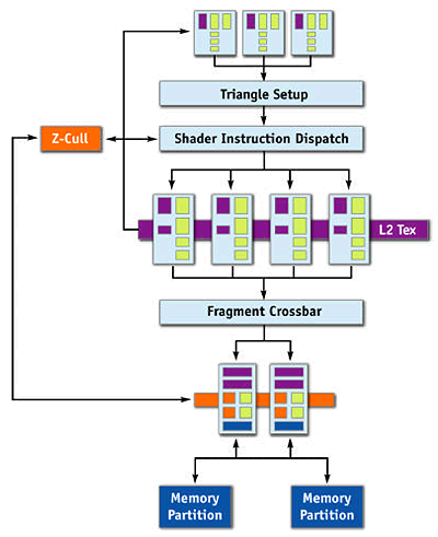
G70 Architecture
The key differences from NV45 are 8 vertex processors and 6 quad processors (all in all, 4*6=24 pixels are processed) instead of 4 with more ALUs for each processor. Pay your attention to the AA, blending, and writing unit, located outside the quad processor on the diagram. The fact is that even though the number of pixel processors is increased by 1.5, the number of modules responsible for writing the results remains the same — 16. That is the new chip can calculate shaders much faster, simultaneously for 24 pixels, but it still writes up to 16 full pixels per clock. It's actually quite enough — memory wouldn't cope with more pixels per clock. Besides, modern applications spend several dozens of commands before calculating and writing a single pixel. That's why increasing the number of pixel processors and retaining the same number of modules responsible for writing looks quite a balanced and logical solution. Such solutions were previously used in low end NVIDIA chips (e.g. GeForce 6200), which had a sterling quad processor, but curtailed writing modules (in terms of the number of units and no FP16 blending). Architecture of the pixel pipeline:
Have a look at the yellow unit of the pixel processor (quad processor). One can say that the architecture used in NV40/45 has been "turboed" — two full vector ALUs, which could execute two different operations over four components, were supplemented with two scalar mini ALUs for parallel execution of simple operations. Now ALUs can execute MAD (simultaneous multiplication and addition) without any penalty.
Adding small simplified and special ALUs is an old NVIDIA's trick, the company resorted to it several times to ensure noticeable performance gain in pixel units by only slightly increasing the number of transistors. For example, even the NV4X had a special unit for normalizing FP16[4] vectors (it is connected to the second main ALU and entitled FP16 NORM on the diagram). The G70 continues the tradition - such a unit allows considerable performance gain in pixel shaders due to free normalization of vectors each time a quad passes though a pipeline of the processor. Interestingly, the normalization operation is coded in shaders as a sequence of several commands, the driver must detect it and substitute it with a single call to this special unit. But in practice this detect process is rather efficient, especially if a shader was compiled from HLSL. Thus, NVIDIA's pixel processors don't spend several clocks on vector normalization as ATI does (it's important not to forget about the format limitation - FP16).
What concerns texture units, everything remains the same — one unit per pixel (that is four units in a quad processor), native L1 Cache in each quad processor, texture filtering in integer or FP16 component format, up to 4 components inclusive (FP16[4]). Texture sampling in FP32 component format is possible only without hardware filtering — you will either have to do without it or program it in a pixel shader, having spent a dozen of instructions or more. However, the same situation happened before - sterling support for FP32 components will probably be introduced only in the next generation of architectures.
The array of six quad processors is followed by the dispatch unit, which redistributes calculated quads among 16 Z, AA, and blending units (to be more exact, among 4 clusters of 4 units, processing an entire quad - geometric consistency must not be lost, as it's necessary to write and compress color and Z buffer.) Each unit can generate, check, and write two Z values or one Z value and one color value per clock. Double-sided stencil buffer operations. Besides, one such unit executes 2x multisampling "free-of-charge", 4x mode requires two passes through this unit, that is two clocks. Let's sum up features of such units:
- Writing colors — FP32[4], FP16[4], INT8[4] per clock, including into different buffers (MRT).
- Comparing and blending colors — FP16[4], INT8[4], FP32 is not supported as a component format
- Comparing, generating, and writing the depth (Z) — all modes; if no color is available — two values per clock (Z-only mode). In MSAA mode — two values per clock as well.
- MSAA — INT8[4], not supported for floating point formats.
There appear so many conditions due to many hardware ALUs, necessary for MSAA operations, generating Z-values, comparing and blending color. NVIDIA tries to optimize transistor usage and employs the same ALUs for different purposes depending on a task. That's why the floating point format excludes MSAA and FP32 excludes blending. A lot of transistors are one of the reasons to preserve 16 units instead of upgrading to 24 ones according to the number of pixel processors. In this case the majority of transistors in these units may (and will) be idle in modern applications with long shaders even in 4xAA mode. Memory, which pass band has not grown compared to the GeForce 6800 Ultra, will not allow to write even 16 full pixels into a frame buffer per clock anyway. As these units are asynchronous to pixel processors (they are calculating Z-values and blending, when shaders calculate colors for the next pixels), 16 units are a justified, even obvious solution. But some restrictions due to FP formats are disappointing but typical of our transition period on the way to symmetric architectures, which will allow all operations with all available data formats without any performance losses, as allowed by flexible modern CPUs in most cases.
Vertex Pipeline Architecture
Everything is familiar by the NV4x family, only the number of vertex processors is increased from 6 to 8.
Details: G71, GeForce 7900 GT/GeForce 7900 GTX/GeForce 7950 GX2
G71 Specifications
- Codename: G71
- Process technology: 90 nm (estimated manufacturer: TSMC)
- 279 million transistors (that is fewer than in G70)
- FC package (flip-chip, flipped chip without a metal cap)
- 256 bit memory interface, four-channel controller
- Up to 1 GB of GDDR3 memory
- PCI Express 16x
- 24 pixel processors, each of them has a texture unit with arbitrary filtering of integer and floating point FP16 textures (including anisotropy, up to 16x inclusive) and "free-of-charge" normalization of FP16 vectors (improved modification of NV4X — more ALUs, efficient MAD execution).
- 8 vertex processors, each of them has a texture unit without sample filtering (discrete sampling).
- Calculating, blending, and writing up to 16 full (color, depth, stencil buffer) pixels per clock
- Calculating and writing up to 32 values of Z buffer and stencil buffer per clock (if no color operations are performed)
- Support for two-sided stencil buffer
- Support for special geometry render optimizations to accelerate shadow algorithms based on stencil buffer and hardware shadow maps (so called Ultra Shadow II technology)
- Everything necessary to support pixel and vertex Shaders 3.0, including dynamic branching in pixel and vertex processors, vertex texture fetch, etc.
- Texture filtering in FP16 format
- Support for a floating point frame buffer (including blending operations in FP16 format and only writing in FP32 format)
- MRT (Multiple Render Targets — rendering into several buffers)
- 2 x RAMDAC 400 MHz
- 2 x DVI interfaces (Dual Link, 2560x1600 support, the interfaces are integrated into G71, so there is no need in external interface chips)
- TV-Out and HDTV-Out are built into the chip
- TV-In (an interface chip is required for video capture)
- Programmable hardware streaming video processor (for video compression, decompression, and post processing), a new generation offering performance sufficient for high-quality HDTV deinterlacing. Sterling hardware acceleration for H.264, WMV-HD, etc.
- 2D accelerator supporting all GDI+ functions
Reference card GeForce 7900 GTX specifications
- Core clock: 650 MHz (pixel processors and blending)
- Vertex Unit Frequency: 700 MHz
- Effective memory frequency: 1.6 GHz (2*800 MHz)
- Memory type: GDDR3, 1.1ns (standard frequency is up to 2*900 MHz)
- Memory: 512 MB
- Memory bandwidth: 51.2 GB/sec.
- Maximum theoretical fillrate: 10.4 gigapixel per second.
- Theoretical texture sampling rate: 15.6 gigatexel per second.
- 2 x DVI-I (Dual Link, 2560x1600 video output)
- SLI connector
- PCI-Express 16x bus
- TV-Out, HDTV-Out, HDCP support
- Power consumption: noticeably lower than in GeForce 7800 (something about 70-80 Watt, but exact figures are not published).
Reference card GeForce 7900 GT specifications
- Core clock: 450 MHz (pixel processors and blending)
- Vertex Unit Frequency: 470 MHz
- Effective memory frequency: 1.32 GHz (2*660 MHz)
- Memory type: GDDR3, 1.4ns (standard frequency is up to 2*700 MHz)
- Memory: 256 MB
- Memory bandwidth: 42.2 GB/sec.
- Maximum theoretical fillrate: 7.2 gigapixel per second.
- Theoretical texture sampling rate: 10.8 gigatexel per second.
- 2 x DVI-I (Dual Link, 2560x1600 video output)
- SLI connector
- PCI-Express 16x bus
- TV-Out, HDTV-Out, HDCP support
- Power consumption: noticeably lower than in GeForce 7800 (something about 50-60 Watt, but exact figures are not published).
Reference card GeForce 7950 GX2 Specifications
- Core clocks: 2 x 500 MHz (pixel processors and blending)
- Vertex unit frequency: 2 x 500 MHz
- Effective memory frequency: 1.2 GHz (2*600 MHz)
- Memory type: GDDR3, 1.4ns (standard frequency is up to 2*700 MHz)
- Memory: 2 x 512 MB
- Memory bandwidth: 2 x 38.4 GB/sec.
- Maximum theoretical fillrate: 2 x 8 gigapixel per second.
- Theoretical texture sampling rate: 2 x 12 gigatexel per second.
- 2 x DVI-I (Dual Link, 2560x1600 video output)
- SLI connector
- PCI-Express 16x bus
- TV-Out, HDTV-Out, HDCP support
- It consumes much more power than GeForce 7800 and 7900 cards (probably more than 100 Watt, exact data are not available).
That's obviously the same architecture as in G70, it's just manufactured by the 90nm process technology with minor changes. For some reason, the number of transistors is noticeably reduced, but it has no effect on performance. Perhaps, G70 had some units in reserve (for example, it might have 7-8 pixel processor quads instead of 6, 9-10 vertex units instead of 8) to increase the yield of effective chips or even to manufacture an Ultra modification, if the competitors had launched a higher-performance model.
To all appearances, a number of units in the new G71 is maximized - either the yield of effective chips manufactured by the 90nm process technology is that high, or NVIDIA can afford more rejects (as the cost of this chip dropped due to its much smaller surface area). There is also another answer to this question - good optimization. But it's less probable, because it's difficult to reduce the number of transistors by 25 millions without any performance loss and preserve the same architecture. But it may be possible, so let's not discard this version from the very beginning. So, there are indirect signs of high yield of effective chips and no manufacturing problems, as well as much lower costs of the new chip compared to G70. Hence the codename - G71, this chip is indeed inferior to G70 in transistors. From the architectural point of view, it offers the same features and the same number of active units. It's all up to the clock frequency, which is much higher here.
Note two integrated Dual Link DVI interfaces - the times of external interface chips are gone. The 400 MHz specifications on RAMDAC are not developed any more - why make it higher, analog monitors have stopped their development. The company declares hardware support for H.264 and other video encoding formats of the latest generations. Interestingly, this feature was also supported by the NV4X family. But some bug made it unavailable to NV40 and NV45. What concerns new chips (NV43, etc), it can be enabled in the new drivers. Along with decoding, we are again promised an improved deinterlacing algorithm and new post processing providing sharper image and better color rendition.
There is an interesting dual-chip modification of G71 - GeForce 7950 GX2 that appeared much later than single-chip cards. In fact, it's two GeForce 7900 GTX chips operating at reduced frequencies in SLI mode on a single card. That is two G71 accelerators operate in a single slot. The price of compact dimensions (compared to two 7900 GTX cards) is reduced operating frequencies, both of memory and of the chips. It's impossible to arrange the chips in a semicircle around the core. So the chips will be at different distances from the GPU, which implies some limitations. Engineers of the dual-GPU card had to use very thin coolers, which limited the range of GPU frequencies, so it was reduced from 650 MHz to 500 MHz. Only the low power consumption and heat release of the G71 chip made it possible to design such a dual-GPU flagship. As neither G70 nor R580 would have allowed to design such a card within the modern PC specifications on power consumption and heat release.
Interestingly, such a card does not require SLI support from a motherboard. Everything necessary is on the card itself. The card consists of two PCBs: master and slave. It's two slots wide. In Quad-SLI mode, the card is connected to the neighboring dial-GPU card via two links. Two components are responsible for SLI: a chip on the second PCB - a modified HSI bridge (PCIE-to-PCIE) and an adapter installed into special connectors on both parts of the card. As a result, we got a compact solution, which can be installed into any standard modern PC case.
If performance of a single GeForce 7950 GX2 card is not enough, you can use two such cards in Quad-SLI mode with a SLI motherboard and a very powerful PSU (support for this mode appeared in Drivers 91.37). Thus, NVIDIA offers a single-card SLI solution as well as an opportunity to upgrade it to Quad-SLI by installing the second card.
It still works as before - there are three cooperative modes - AFR (Alternative Frame Rendering), Slicing (splitting a frame into four zones) and SLI-AA - using accelerators to calculate different AA samples in a single pixel. Besides, it's logical to combine the modes - for example, 2xAFR from two two-zone frames (Alternative Frame Rendering, where each frame is formed by SLI slicing) or 2x SLI-AA slicing, etc. There can be many combinations, but no new architectural changes are necessary - SLI already offers many features, their combinations are controlled by the driver.
Details: G73, GeForce 7600 GT/GeForce 7600 GS
G73 Specifications
- Codename: G73
- Process technology: 90 nm (estimated manufacturer: TSMC)
- 178 million transistors
- FC package (flip-chip, flipped chip without a metal cap)
- 128 bit memory interface (dual channel controller)
- Up to 512 MB of GDDR3 memory
- PCI Express 16x
- 12 pixel processors, each of them has a texture unit with arbitrary filtering of integer and floating point FP16 textures (including anisotropy, up to 16x inclusive) and "free-of-charge" normalization of FP16 vectors (improved modification of NV4X — more ALUs, efficient MAD execution).
- 5 vertex processors, each of them has a texture unit without sample filtering (discrete sampling).
- Calculation, blending, and writing of up to 8 full (color, depth, stencil buffer) pixels per clock
- Calculating and writing up to 16 values of Z buffer and stencil buffer per clock (if no color operations are performed)
- Support for two-sided stencil buffer
- Support for special geometry render optimizations to accelerate shadow algorithms based on stencil buffer and hardware shadow maps (so called Ultra Shadow II technology)
- Everything necessary to support pixel and vertex Shaders 3.0, including dynamic branching in pixel and vertex processors, vertex texture fetch, etc.
- Texture filtering in FP16 format
- Support for a floating point frame buffer (including blending operations in FP16 format and only writing in FP32 format)
- MRT (Multiple Render Targets — rendering into several buffers)
- 2 x RAMDAC 400 MHz
- 2 x DVI Dual Link interfaces (2560x1600 support, the interfaces are integrated into G73, so there is no need in external interface chips)
- TV-Out and HDTV-Out are built into the chip
- TV-In (an interface chip is required for video capture)
- Programmable hardware streaming video processor (for video compression, decompression, and post processing), a new generation offering performance sufficient for high-quality HDTV deinterlacing. Sterling hardware acceleration for H.264, WMV-HD, etc.
- 2D accelerator supporting all GDI+ functions
Reference card GeForce 7600 GT specifications
- Core clock: 560 MHz (pixel processors and blending)
- Vertex Unit Frequency: 560 MHz
- Effective memory frequency: 1.4 GHz (2*700 MHz)
- Memory type: GDDR3, 1.4ns (standard frequency is up to 2*700 MHz)
- Memory: 256 MB
- Memory bandwidth: 22.4 GB/sec.
- Maximum theoretical fillrate: 4.48 gigapixel per second.
- Theoretical texture sampling rate: 6.72 gigatexel per second.
- 2 x DVI-I (Dual Link, 2560x1600 video output)
- SLI connector
- PCI-Express 16x bus
- TV-Out, HDTV-Out, HDCP support
- It consumes very little power (something about 40-60 Watt, but exact data are not available).
Reference GeForce 7600 GS Specifications
- Core clock: 400 MHz (pixel processors and blending)
- Vertex Unit Frequency: 400 MHz
- Effective memory frequency: 0.8 GHz (2*400 MHz)
- Memory type: DDR2, 2.5ns (standard frequency: up to 2*400 MHz)
- Memory: 256 MB
- Memory bandwidth: 12.8 GB/sec.
- Maximum theoretical fillrate: 3.2 gigapixel per second.
- Theoretical texture sampling rate: 4.8 gigatexel per second.
- 2 x DVI-I (Dual Link, 2560x1600 video output)
- SLI connector
- PCI-Express 16x bus
- TV-Out, HDTV-Out, HDCP support
- Power consumption: lower than in GeForce 7600 GT
G73 is evidently a half (except for 5 instead of 4 vertex units) of G71. Both in terms of the memory controller as well as the pixel part. But we should make a reservation here - according to our tests, G73 physically has 16 pixel processors, not 12 (that is it has 4 quads). One quad is retained to increase the yield of effective chips or (you never can tell) for a future solution with 16 pixel units to oppose a new competitor on the market. The surface area of the chip is smaller than in NV43, but the chip is much more efficient.
G74 codename is not used yet - to all appearances, it can be used for a cheaper G71 reincarnation. It can also be designed for 20 or 16 pixel pipelines.
Details: G72, GeForce 7300 GS
G72 Specifications
- Codename: G72
- Process technology: 90 nm (estimated manufacturer: TSMC)
- 112 million transistors
- FC package (flip-chip, flipped chip without a metal cap)
- 64 bit memory interface (dual channel controller)
- Up to 512 MB of DDR2/GDDR3 memory
- PCI Express 16x
- 4 pixel processors, each of them has a texture unit with arbitrary filtering of integer and floating point FP16 textures (including anisotropy, up to 16x inclusive) and "free-of-charge" normalization of FP16 vectors (improved modification of NV4X — more ALUs, efficient MAD execution).
- 3 vertex processors, each with a texture unit, without filtering samples (discrete sampling).
- Calculating, blending, and writing up to 2 full (color, depth, stencil buffer) pixels per clock
- Calculating and writing up to 4 values of Z buffer and stencil buffer per clock (if no color operations are performed)
- Support for two-sided stencil buffer
- Support for special geometry render optimizations to accelerate shadow algorithms based on stencil buffer and hardware shadow maps (so called Ultra Shadow II technology)
- Everything necessary to support pixel and vertex Shaders 3.0, including dynamic branching in pixel and vertex processors, vertex texture fetch, etc.
- Texture filtering in FP16 format
- Support for a floating point frame buffer (including blending operations in FP16 format and only writing in FP32 format)
- MRT (Multiple Render Targets — rendering into several buffers)
- 2 x RAMDAC 400 MHz
- DVI Dual Link supporting up to 2560x1600 video output, this interface is integrated into the chip, so an external interface chip is not necessary)
- TV-Out and HDTV-Out are built into the chip
- TV-In (an interface chip is required for video capture)
- Programmable hardware streaming video processor (for video compression, decompression, and post processing), a new generation offering performance sufficient for high-quality HDTV deinterlacing. Sterling hardware acceleration for H.264, WMV-HD, etc.
- 2D accelerator supporting all GDI+ functions
Reference GeForce 7300 GS Specifications
- Core clock: 550 MHz (pixel processors and blending)
- Vertex Unit Frequency: 550 MHz
- Effective memory frequency: 0.7 GHz (2*350 MHz)
- Memory type: DDR2, 2.8ns (standard frequency: up to 2*350 MHz)
- Memory: 256 MB
- Memory bandwidth: 5.6 GB/sec.
- Maximum theoretical fillrate: 1.1 gigapixel per second.
- Theoretical texture sampling rate: 2.2 gigatexel per second.
- Support Dual Link DVI-I, 2560x1600 video output
- PCI-Express 16x bus
- TV-Out, HDTV-Out, HDCP support
- Power consumption: very low
This G7x-series modification has even fewer units - only four pixel processors and four texture units, three vertex processors, and two ROPs. In other respects, the card is just like the other models in the family from other price segments, the architecture is practically the same. There may be some changes in cache sizes and the like, but we cannot say anything more specific, we can only speculate.
Interestingly, later on there appeared GeForce 7300 GT card, it wasn't based on G72, as you might have assumed; it was based on the de-featured and slowed-down G73, that is on the chip used in the GeForce 7600 series. But the chip was reduced from 12 pixel units to 8. And it has one active vertex unit down. I wonder why this card hasn't been called GeForce 7600 LE or XT. This name would have been much better.
Alexei Berillo aka SomeBody Else
(sbe@ixbt.com)
Updated: August 14, 2006
Write a comment below. No registration needed!
|
|
 |
|
|
|