 |
||
|
||
| ||
|
||
|
||
| ||
Part 1. Theory and architecture
 No secret that ATI delayed the launch of a new generation of video accelerators. We don't know for sure whether it was due to the new process technology (90 nm) and attempts to design the R520 revision to provide necessary frequencies and yield of effective dies, or other reasons (for example, forced lull on the graphics market in terms of new products before the release of Vista and accelerators complying with WGF 2.0 paradigm). But the fact remains, the competing product from NVIDIA appeared earlier and we already had time to examine it, having drawn a definite conclusion on the evolutional rather than revolutional character of the G70 versus the NV4X series. As we already know (from our preview as well), this situation is different: a different process technology and a different architecture. The series comprises three new accelerators — high-performance R520, middle end RV530, and budget RV515. Meet Shaders 3.0 from ATI — with a quality status stamp. Official RADEON X1800 Specifications
Official RADEON X1600 Specifications
Official RADEON X1300 Specifications
We shall analyze the new ATI architecture later on, but now we are going to point out the most important moments: all-round SM3 support including the efficient branching, operations with FP16 storage and rendering formats without any limitations (as well as integer formats, including MSAA and texture compression), FP32 calculating precision inside the chip. The new series of video cards
It goes without saying that there will later appear new reference configurations and new cards from ATI. As for now, we shall note a delay, nearly to December, in the availability of RV530-based products (this chip was developed later than the R520; it features some of the traits of the future R580, hence the delay with mass production) an of the top product in this series — X1800 XT. That's a bit disappointing, it means that the fastest accelerator will be most likely a press-card for nearly a whole month (reviewers got their samples by the announcement time), intended to compete with the G70 in reviews rather than on the store shelves. That may be the fault of the yield of effective chips or some other reasons, but we shall not see this card on the shelves until the 5th of November. Taking into account the high competition potential of the RV530 and the chances of the 1800XT to outperform the GeForce 7800 GTX, we can just lament these delays — it would have been much better, if all the products of the new series, long-expected by ATI fans, had appeared in stores right now. R520 ArchitectureWe are not going to publish our own diagram this time. Instead, we'll provide an ATI scheme — it offers a praiseworthy detailing level and shows all necessary issues. Let's have a closer look: 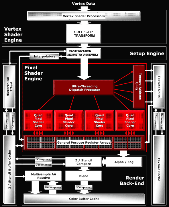 Architecture of vertex processorsThere are 8 identical vertex processors (they are inside the Vertex Shader Processors unit on the diagram). They comply with SM3 requirements and are based on ATI's standard 3+1 scheme (ALU of each vertex processor can execute two different operations simultaneously over three vector components and the fourth component or a scalar). In fact, vertex processors have become similar to what we saw in the NV4X and the G70, for the only exception — they offer the 3+1 scheme instead of 4+1 (those processors could process a 4-component vector and a scalar). The G70 scheme can potentially offer higher performance, but the real difference may be practically unnoticeable, especially in our times, when vertex processors rarely act as a rendering bottleneck. Later on we shall investigate (and test) the question of the implementation and efficiency of texture access from ATI vector processors. Architecture of the pixel partThat's where the most interesting things are hidden. Have a look at the diagram above — unlike NVIDIA, the texture units are outside the common pipeline. The chip architecture may be called distributed — there is no common long pipeline to run quads through, as in case of NVIDIA. The texture part exists separately — texture address units and TMUs. Pixel processors (performing arithmetic and other operations) and register arrays stand separately. This scheme has its pros and cons. The main disadvantage — it suits well the phase mechanism, when active texture sampling precedes texture calculations (Shaders 1.X and old programs with stages), bit it is fraught with unjustified latencies in dependent texture samples, which can be often found in modern Shaders 2.X and 3.0. Think about it — one texture access command really calls a lengthy operation for many cycles and the shader processor should stand idle for all this time? Nothing of the sort — ATI settles the point rather smartly! Moreover, this solution is universal, not only does it effectively execute dependent samples, it also increases efficiency of the pixel part in shaders with conditions and branches (compared to NVIDIA's approach). ATI calls this technology hyper threading. OK, how does it work? The magic box (Ultra Threading Dispatch Processor) directs the execution — it processes 512 quads simultaneously, each of them can be at a different shader execution stage. Each quad is stored together with its current status, current shader command, values of previously checked conditions (information on the current branch of a conditional jump). NVIDIA chips run quads in circle, one after another. Maximum they can do is to skip quads, which don't fall under the current branch of a condition. The R520 operates differently — our magic box constantly monitors free resources (be it texture or pixel units) and directs queued quads into free devices. If a quad fails a condition and should not be processed by this or that shader part, it will not hang about in circles, taking up room and time, together with the other quads, which need to be processed. It will just skip unnecessary commands and will not load a texture or pixel unit. If a quad waits for data from a texture unit — it will let other quads forward, which will load pixel units for this time. Thus, this approach kills two birds with one stone — it hides texture access latency and allows efficient usage of computing and texture resources when shaders with conditions and branches are executed. Efficiency of both issues depends directly on the number of quads that our magic box can process. 512 look like an imposing set (we can get textures for 4 quads and process 4 quads in pixel processors per cycle; thus up to 8 quads are processed each cycle, while the rest of the quads wait for their turn or wait for data from texture units). This unit is undoubtedly complex and the dispatching logic for this quad set takes up a considerable part of the chip, probably comparable with texture and pixel processors. Especially as register arrays actually belong to this unit as well — there must be lots of them to store efficiently all preliminary calculations for the 512 quads in queue. Now what concerns pixel processors and ALU. As we have already seen, pixel processors are grouped in four — that is we actually have four quad processors processing four pixels per cycle rather than 16 separate processors. Each such quad processor consists of the following units: 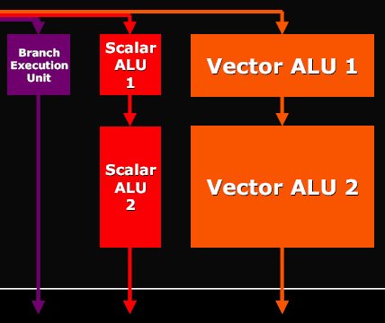 and can execute the following operations over four pixels per cycle:
Don't forget that except for these five operations, a texture address operation can be executed in parallel (that is requesting data from TMU). Thus, in case of optimal shader code, we got the peak performance of 6 operations per cycle, which is (theoretically) comparable with the G70, taking into account the difference in architectural approaches to branching. But as we have already mentioned above, the scheme from ATI is better at branching. We shall test this assumption in practical tests. Interestingly, ATI is true to its approach — 3+1 (two different operations can be executed, one - over three components of a vector, the other - over a scalar, being the fourth component). In the majority of cases, the approach taken by NVIDIA (an option of 2+2 or 3+1) can be considered more efficient, but this difference will have a little effect on typical graphics tasks. Another major issue of the new architecture — caching compressed data — both Z / Frame buffer values and texture data are stored in caches in compressed form. They are decompressed on the fly, when they are accessed from the corresponding units. Thus the caching efficiency grows higher. You can say that the cache sizes are virtually increased several-fold. It would be logical to assume that such an architecture with separated texture and pixel units will be easily scalable: 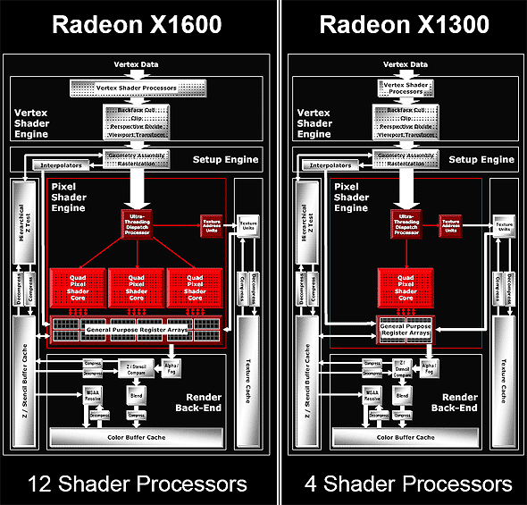 As we can see, RV530 and RV515 are built on the same scheme. There is only one quad left in the RV515 — it simplifies many aspects, including the magic box of the dispatcher. The situation with the RV530 is more complex — it has three pixel quad processors, but only one texture unit. As a result, we have 12 pixel processors and 4 TMUs, even if used in the optimal way, nearly without downtime. Of course, in case of simple shaders without complex calculations, pixel processors will be idle waiting for texture data. But modern shaders, for which this chip is intended, are often up to much calculations (5-8 commands) per one texture access, justifying this scheme. To all appearances, the number of transistors spent on the texture part of the chip is greater than in case of pixel ALUs. That's why this disbalance is justified from the point of view of ATI designers. In fact, giving up 6-8 texture units allows 12 (instead of 8 or 4) pixel processors, keeping the same complexity of the chip. How justified it is in practice depends on the efficiency of ATI texture units (that's what the designers pin their hopes on), on the efficiency of the dispatcher, and on the ratio of various commands in executed shaders. It's hard to guess, we shall check up on this aspect in our practical section with various tests. But now we shall just warm your interest to the question — whether the ATI's move is justified and how it will affect the competition with NVIDIA, especially in the light of the awaited soon 12-pipeline G70 (G72). On output interfacesThe new accelerators support HDCP format for both DVI interfaces. Senior R520-based models are capable of applying HDMI (High Definition Media Interface, the interface for outputting video and audio to digital theatres and other audio-video playback devices of the new generation) to DVI connectors. You can learn more details on popular interfaces in our R520 preview. Conclusions
Stay with us, the continuation will follow soon :-)
Write a comment below. No registration needed!
|
Platform · Video · Multimedia · Mobile · Other || About us & Privacy policy · Twitter · Facebook Copyright © Byrds Research & Publishing, Ltd., 1997–2011. All rights reserved. |


