|
||
|
||
| ||
|
||
|
||
| ||
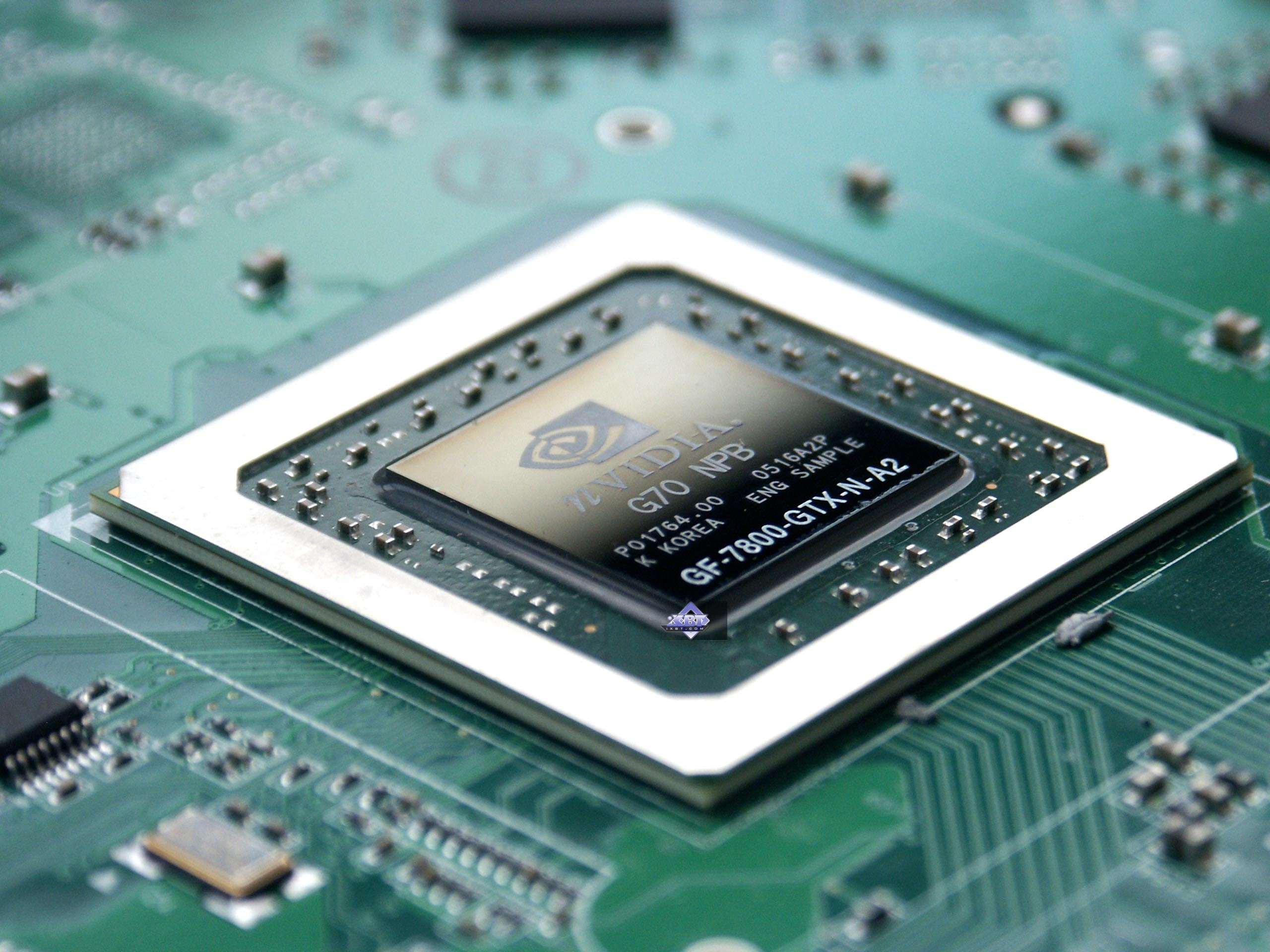 TABLE OF CONTENTS
NVIDIA GeForce 7800 GTX 256MB PCI-E: Part 1: Theoretical materialsWe have already reviewed theoretical aspects of the architecture of the new product from NVIDIA in the previous parts. In this section we are going to examine the card itself that represents a new GPU. We shall also see what performance GeForce 7800 GTX demonstrates in synthetic tests. In the third part we shall see the most important thing for all gamers — 3D performance. The article will be concluded with a small section about the AA quality (we shall examine new modes). So, let's have a look at the reference card.
Video card
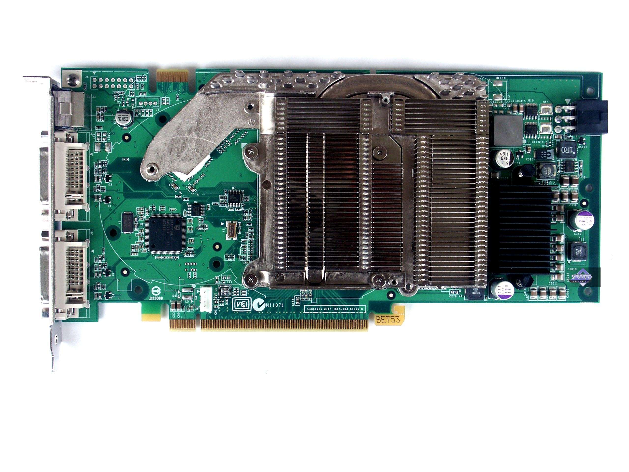
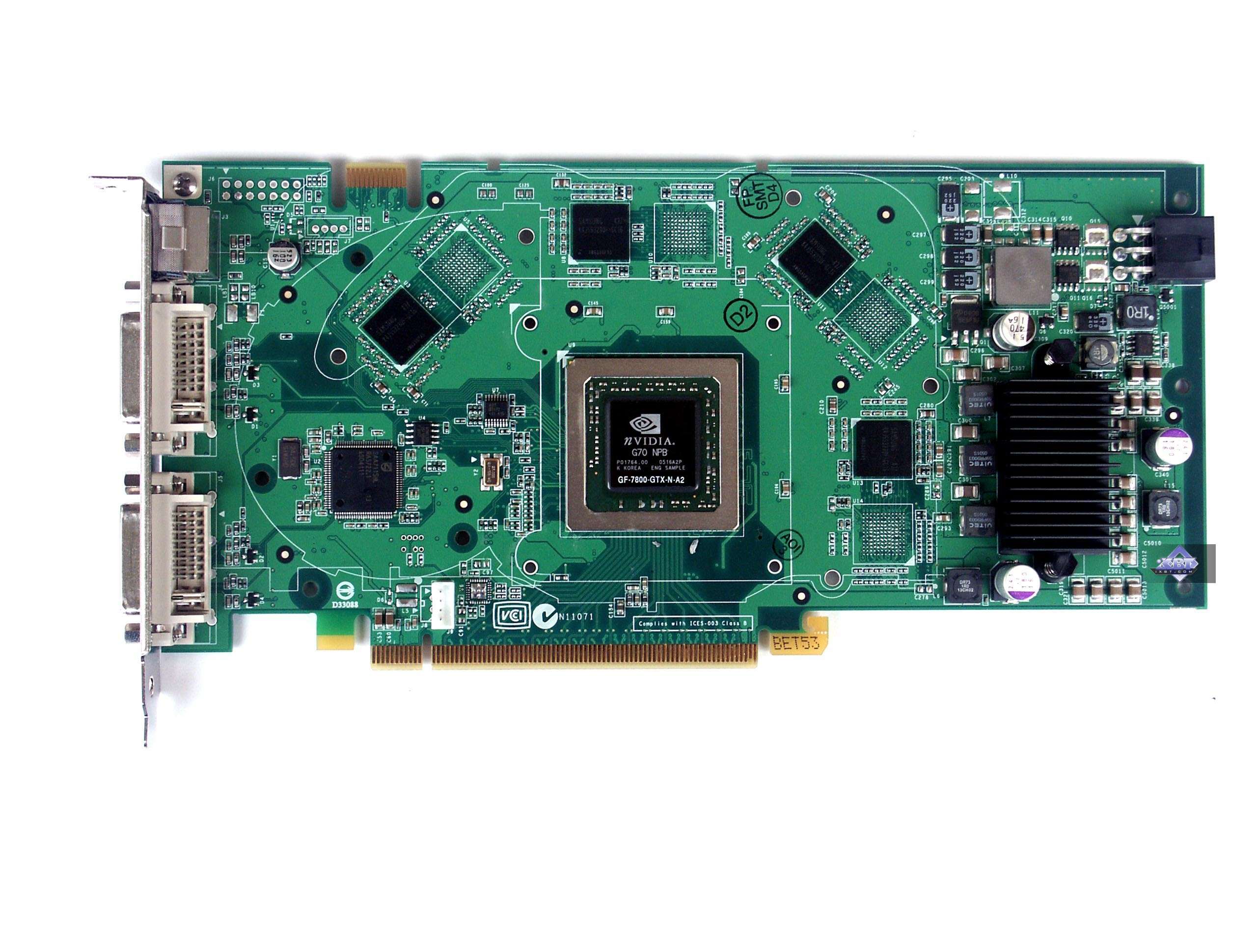
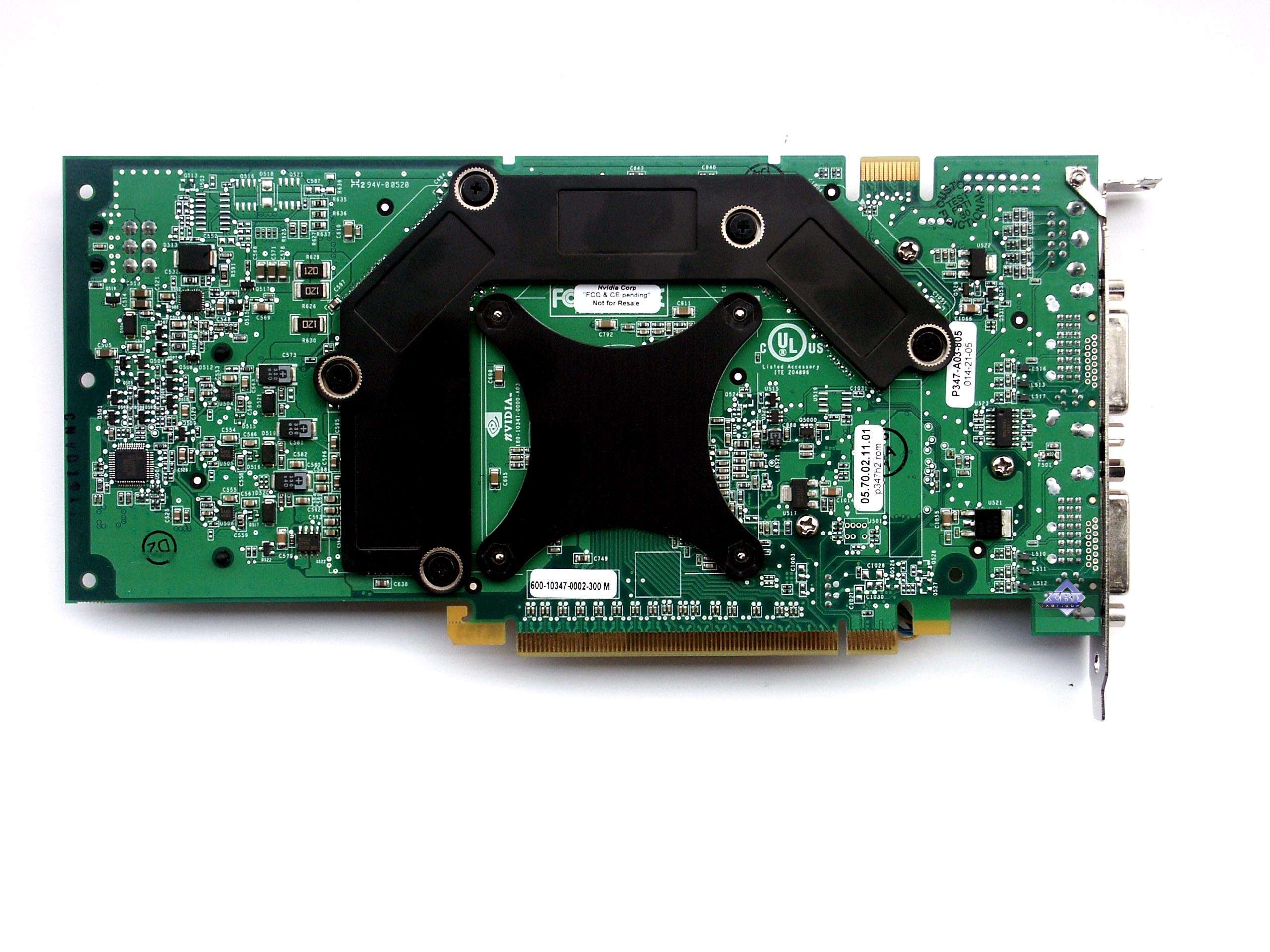
This card is obviously designed after the previous card, it generally resembles a card on NV45 (GeForce 6800 GT/U). Changes mostly concern the power section. The power supply unit is considerably overhauled. We can also see that the PCB is designed for 16 memory chips, so the same board can be used for 512MB modifications of the product. Only half of memory chips (256MB) is installed in this case. Note that the chips are installed next but one (it's not that all the chips are installed on the front side of the PCB leaving the back side empty, which would be more logical), so they are scattered on both sides. The product has VIVO, where VideoIn is based on Philips 7115. The whole last year we were surprised why the entire GeForce 6800 series was not equipped with such coders, though PCBs provided empty seats for them. Nobody could explain why none of NVIDIA's partners installed such a chip on its cards. There probably were some layout defects. And now a video input is good news.  We should also mention that the card is equipped with a couple of DVI connectors. Now what concerns the cooling system. I have published a photo of the card with cooler housing removed on purpose. You can see that much has been modified in this cooler, though it resembles the old reference cooler. 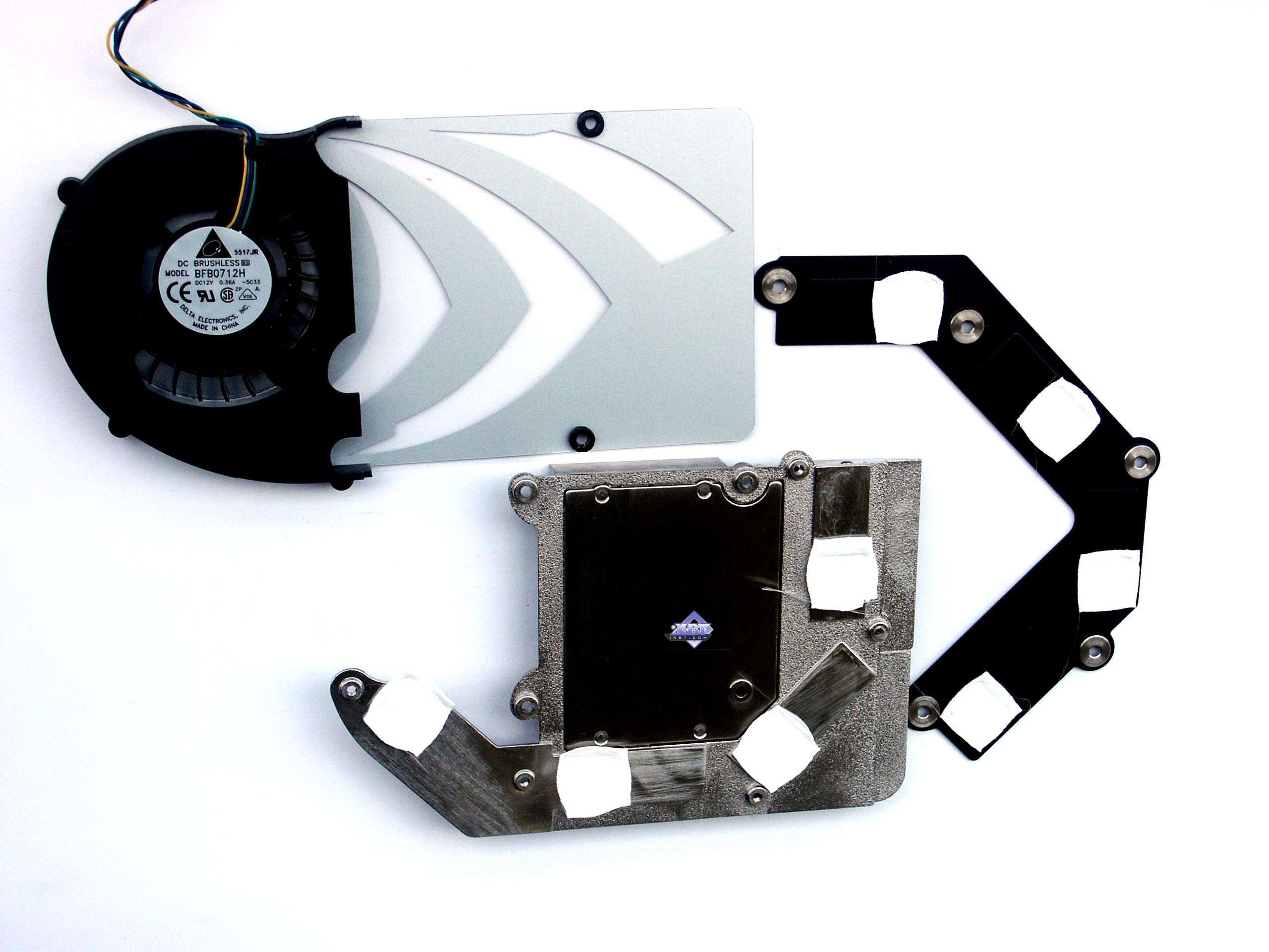   First of all you can see that the central heatsink is now connected to the memory heatsink with a heat pipe. Then, the device is rather slim, it takes up only a single slot, which is good news (we are tired of bulky accelerators). Memory chips on the back of the PCB are cooled by a narrow plate. On the whole, the cooler is not noisy. Only the first seconds after startup are a tad noisy because of the high rpms of the turbine. You can hear the noise in this video (1.5MB, WMV) (note that the turbine does not start up immediately after the computer is turned on). Now have a look at the processor.  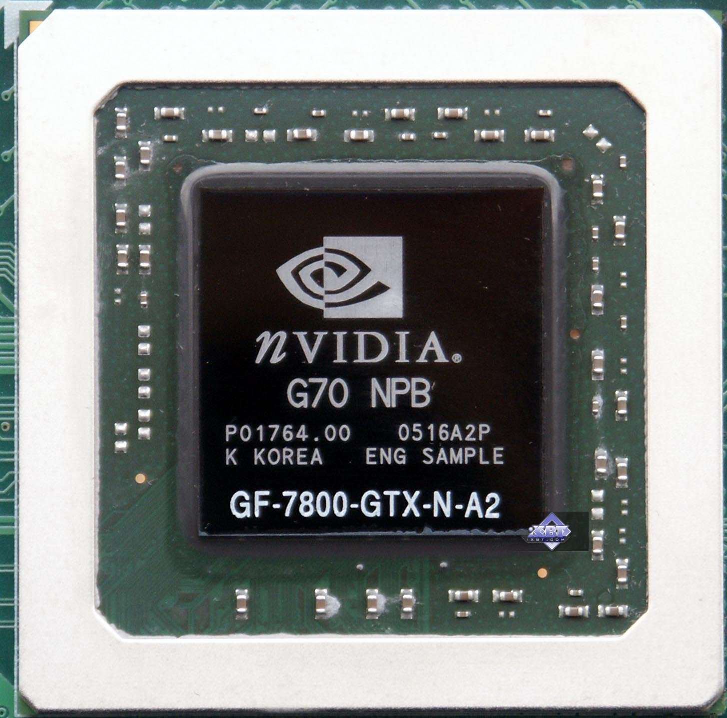 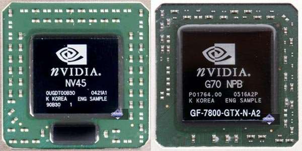 The third photo compares G70 with its predecessor. What do we see? Although the process technology is thinner, 300 million transistors make themselves felt — the die surface has grown larger. Not long ago we groaned about the large NVIDIA's chip... And now it's even larger :). According to its designation, the chip is manufactured or packaged in Korea. That's confusing. It's well known that TSMC has its own facilities for packaging dies, that's why the die should have been stamped TAIWAN, if manufactured by TSMC. There is a packaging plant in Korea, but it mostly processes dies from IBM. Has the American blue giant taken up NV47\G70 manufacturing again? The matter is left open. And the final issue that has to do with the card itself: dimensions. Note that it's currently the longest card among modern accelerators. You can see it well on the photo: 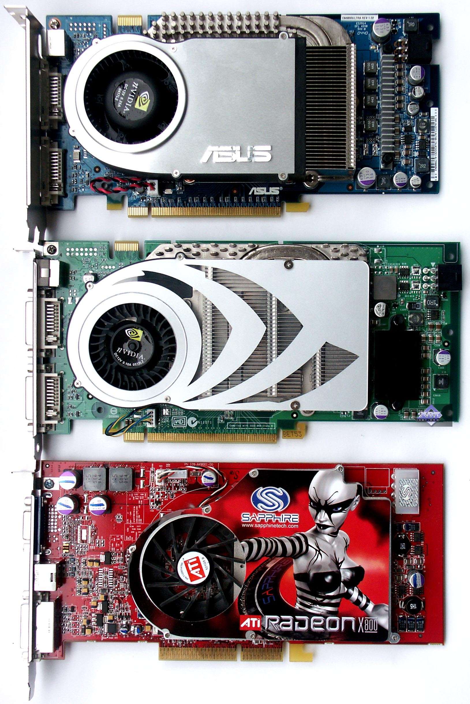 The 6800 Ultra is on top — it used to be the largest accelerator. But there appeared the RADEON X800 AGP not long ago, which is on the photo below, and it became the longest card. Now it takes a second place, because the 7800 GTX turns out the longest now. You should keep it all in mind, as there are a lot of chassis that simply cannot accommodate this card (in my case, I had hard times squeezing the 6800 Ultra into ThermalTake Xazer II, I had to install HDD higher or lower than the card, they just wouldn't fit on the same level). In conclusion of this section I'd like to publish some more photos. :) As you already know, we have actually tested two cards in SLI mode:    These photos will also help you size up the cards, especially their thickness.
Installation and DriversTestbed configurations:
VSync is disabled. A few words about the drivers. New Version 77.62 already supports NV47 (G70). I'll explain why NV47 below.   It's drivers (settings) for the G70 series that now allow to enable TAA (MSAA, SSAA), and gamma-correction in AA. Read the third part of the article to learn more details on the new AA modes. Thanks to the responsiveness of the author of RivaTuner (A.Nikolaychuk AKA Unwinder), beta-version 15.6 already supports the GeForce 7800: 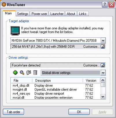 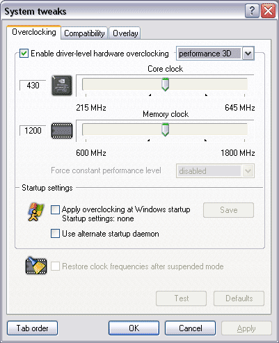 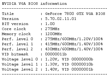 As you can see, the program detects the chip as NV47 not as G70. The fact is that the chip registers retain this codename — NV47, that is the chip announces itself as NV47 not as G70. That's why the program retains this codename as well. Using the NVStrap driver we can easily reduce the number of active pipelines. We did it to configure the chip to have 16/6 pipelines, in order to compare it with NV45 (having reduced the frequencies to 425/1100 MHz). Temperature monitoring works well as well. I want to note that the chip gets heated to 80 degrees without additional cooling, which is comparable with the 6800 Ultra, that's quite all right.  But we must note that the entire card gets very hot, you cannot even touch the back of PCB. Memory heatsinks are also very hot. There is just a chance that the memory operates at the increased voltage. We have no other explanations for the sudden overclocking capacity up to 1400 MHz, while it could hardly reach the standard 1250 MHz before. Probably the updated PCB plays its role. Speaking of overclocking: the chip can now operate at 495 MHz (probably even at 500 MHz, but I had no time to analyze the card's operation at higher frequencies). Even drivers allowed it during frequency tests (you are sure to know that designers are always overcautious as far as overclocking is concerned). Thus, we can ascertain an excellent overclocking potential of the new GPU (despite the new process technology. Mind it that the R430, manufactured by the same 0.11-micron process technology, is very bad at overclocking). That's why the launch of the future GeForce 7800 Ultra already looms in the distance.
Synthetic testsD3D RightMark Beta 4 (1050) and its description (used in our tests) are available at http://3d.rightmark.org Here are the D3D parameters: D3D RightMark: G70, NV4X, R4XX We carried out our tests with the following cards:
Besides, we ran our synthetic tests in a SLI configuration to control anomalies. We shall not publish these results here for they are useless — as is well known, video efficiency in SLI mode depends much on a given application and you cannot forecast judging from synthetic tests — the data does not correlate with game results. So, let's proceed: Pixel Filling testPeak texelrate, FFP mode, various numbers of textures applied to a single pixel: 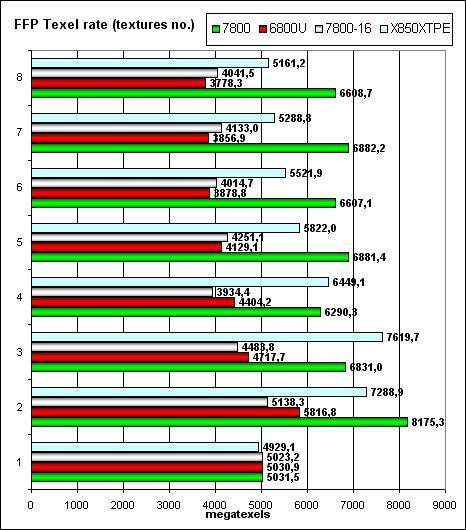 Higher core clock and 24 pipelines make themselves felt - now NVIDIA leads even in traditionally weak (compared to ATI) situations. It's interesting to see how the dependence on the number of textures is changed in the 7800-16 mode (the same frequencies and pipeline numbers as in the 6800U). Perhaps, the latency, granularity, and cache sizes, as well as the algorithm of operations with them were changed; the balance shifted to more textures — that is the NV47/G70 architecture is preferable for complex tasks. And now what concerns the fillrate and pixelrate of a frame buffer, FFP mode, for various number of textures applied to a single pixel: 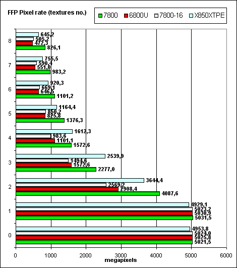 It happens so fast in a single texture mode (with a fixed color), that it's limited by writing and blending units (16 units both in NV40/45 and in G70). That's why the results are the same with a small number of textures. With two or more textures, the chip gets a chance to use all its 24 texture units — have a look at the abrupt leap. Even the frame buffer of the X850, which is traditionally faster in fillrate (without extra calculations), is no longer a leader and is sometimes defeated by the G70 as the number of textures grows (this tendency speaks of larger caches in the NVIDIA products compared to ATI). Let's see how the fillrate depends on a shader version (1.1): 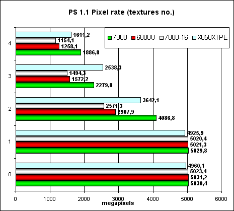 the same picture as in case of FFP, and Version 2.0: 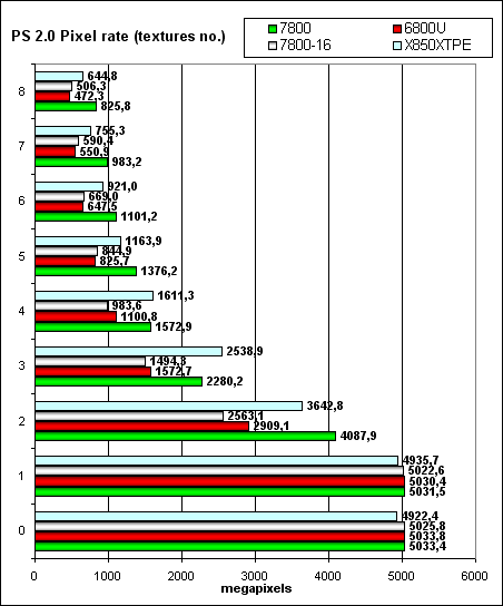 Using different shader versions has almost no effect on performance now — NV3X strange oddities sank into oblivion and the results are expectable and linear — all shader versions being physically executed in the same way, on the same pixel processors. So, we can establish the following facts:
Geometry Processing Speed testThe simplest shader — maximum bandwidth in terms of triangles: 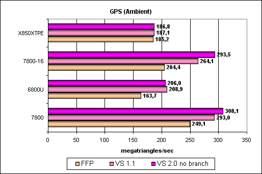 So, the G70 is certainly the new leader, its peak performance scales well together with the core clock and the number of pipelines. Interestingly, geometry processors in the G70 are more effective than those in the NV45, even though they operate at the same frequency. How come, we were promised the same thing without changes? The answer probably lies in intermediate caches for geometry content and the higher sample and transfer efficiency. Let's check this assumption with more complex tests. A more complex shader — a single plain spotlight: 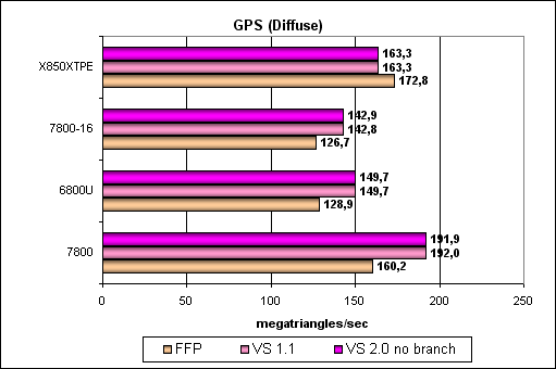 Aha! That's OK, the difference between G70 and NV45 at equal frequencies and with the same number of pipelines disappears — the problem was really in the buffers and geometry sampling. No surprises, the G70 is the leader, its full performance is proportionally higher than in the NV45, considering a higher clock and 8 vertex units instead of 6. Let's complicate the task:  A similar picture. And now the most difficult task: three light sources. We also included options without branching, with static and dynamic branching: 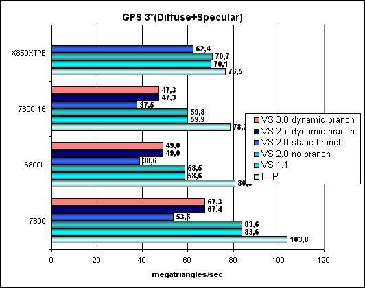 FFP is strong, static branching is a noticeable blow to NVIDIA chips. The paradox is that dynamic branching is better than static in NVIDIA chips. In case of ATI everything is even, FFP is almost on a par with shaders. We can see no architectural innovations, the G70 is just an overclocked NV45 in this respect, all the dependencies remained the same. According to NVIDIA, the new generation of video chips has an improved rasterizer. It was necessary to avoid the rasterizer bottleneck in the architecture of the video chip so that it would manage to process all triangles, transformed by the eight vertex shaders. One of the indirect signs of this improvement is a modified size of Post-VS Cache, placed after vertex shaders before the rasterizer. This cache may hold a certain number of vertices processed by vertex shaders. The number of cached vertices does not depend on the number of attributes (colors, texture coordinates), calculated in a vertex shader. When the rasterizer processes neighboring triangles with common vertices, vertex shaders don't have to recalculate these vertices. Let's have a look at the triangle rasterization rate depending on the number of vertices: 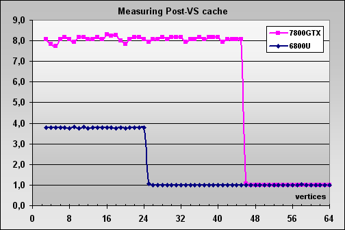 ATTENTION: the graph was scaled to reflect the ratio between the triangle rasterization rate and the vertex transformation rate in different generations of NVIDIA chips. You can see that Post-VS has grown from 24 to 45 vertices and that NVIDIA engineers have increased the rasterization rate higher than required by vertex shaders increased from 6 to 8. When all vertices necessary for rasterization are already cached, the triangle processing rate grows by 8 times! This solution again speaks of the balance shifted to more complex scenes, in this case — to more complex geometry models, consisting of a lot of smaller triangles. That is models with more details. Another interesting fact: when the driver requests the Post-VS Cache size of GeForce 7800, it returns the same value of 16 vertices as in case of GeForce 6800. We don't know whether it's a defect or a deliberate act to preserve compatibility. Below is a table with Post-TNL / Post-VS Cache sizes in various generations of NVIDIA video chips.
So,
Pixel Shaders TestThe first group of shaders, which is rather simple to execute in real time, 1.1, 1.4, and 2.0: 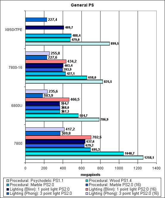 Considering a higher clock and 24 pipelines, the G70 is a definite leader. However, comparing it with the NV45 one-to-one makes it clear that although pixel pipelines were improved, as we mentioned in the theoretical part of the article, there is practically little help from these improvements, at least in our synthetic tests. "Boring cylinders" is faster, but not so radical, there is no difference at all in some tests. Well, at least it's not slower, that's what important — more pipelines and a higher overclocking potential pardon no architectural innovations. As usual, the American marketing department of NVIDIA has shed too much peachy details on this minor tuning of pixel pipelines — to all appearances, twofold gain in shader execution speed in common applications is out of the question. 1.5-fold gain is out of the question as well. Let's see what will change in case of more complex shaders:  No, the picture is the same. Our tests reveal only a minor advantage of the new optimized pixel pipelines. Considering quite a typical shader code of these tests, we can assume that there is no strong advantage in game applications as well. However, let's not jump at conclusions until the next part of the article, where we shall confirm or disprove it in practice. Bottom line under pixel shaders:
HSR testPeak efficiency (with and without textures) depending on geometry complexity: 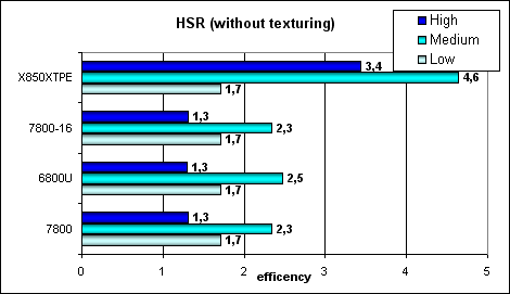 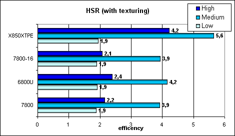 You can see that ATI is doing better at average and complex scenes — that's the effect of two levels of reduced Z buffers (besides the basic buffer). NVIDIA traditionally offers one additional level, that's why the HSR efficiency is noticeably lower, in case of the optimal scene balance (average complexity). We can see that the HSR algorithm is not changed — the efficiency of G70 and NV45 is on the same level — the difference is within the measurement error. It means that the ratio of truncated and filled pixels per cycle is not changed. But the absolute figures are considerably higher, taking into account 24 pipelines. Conclusion:
Point Sprites test.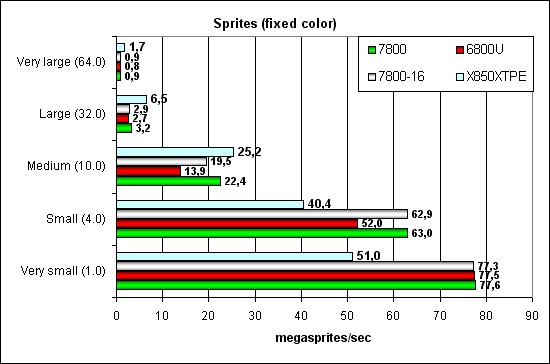 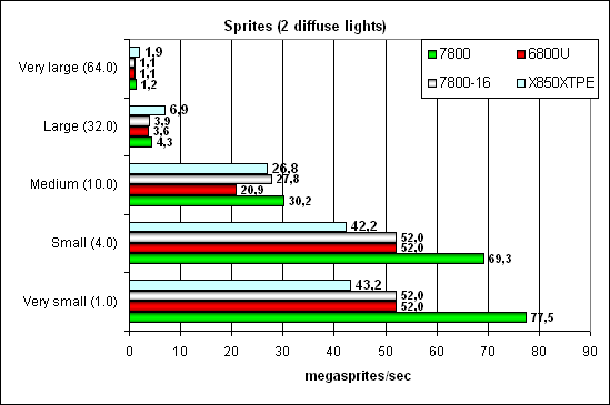 Sprites have gone out of popular innovations long ago, they are often slower than triangles in output rate. Anyway, ATI used to be better at small and medium sprites and now G70 leads (large sprites make little sense — polygons are better in this case). But that's due to brute force — the balance is not changed — the algorithm is the same. Interestingly, the modification with 16 pipelines is still noticeably faster than NV45 — probably there are units responsible for some aspects of sprite operations, and their number is not reduced after pixel pipelines were cut down to 16 and vertex pipelines - to 6. MSAA testWe don't publish the results of this test, as there are no architectural differences from NV45, even the efficiency is the same — the effect of 16 writing and blending units in both chips. We'll just repeat the conclusion we made from the comparison of R420 and NV40: NVIDIA is more efficient in the peak MSAA case. The drop is lower in case of 4x. But NVIDIA's antialiasing is of a lower quality. One can see well that 8x in NV40 is a hybrid setup with SSAA — the speed drops below the admissible level. But then, MSAA 6x is practically no different from 4x (in R4XX family) in terms of performance, a welcome issue. In the third part of the article we shall examine performance, quality, and rates of the new AA mode with transparent polygons. Conclusions on the synthetic tests
NVIDIA GeForce 7800 GTX 256MB PCI-E: Part 3: Game tests, new AA types, conclusions.
We express our thanks to Alexei Barkovoy for his help and valuable advice Andrey Vorobiev (anvakams@ixbt.com) Alexander Medvedev (unclesam@ixbt.com) June 22, 2005. Write a comment below. No registration needed!
|
Platform · Video · Multimedia · Mobile · Other || About us & Privacy policy · Twitter · Facebook Copyright © Byrds Research & Publishing, Ltd., 1997–2011. All rights reserved. | ||||||||||||||||||||||||||||||||||||||||||||||||||||||||||||||||||||||||