 |
||
|
||
| ||
On April 14 Intel plans to announce a new Pentium 4 processor clocked at 3.0GHz though a model running at 3.06GHz was released over half a year ago. The real difference is the FSB speed which makes 800 MHz. So, a year after the Pentium 4 shifted to the 533MHz bus, this line has made one more expected step increasing the FSB's rate by 50%. 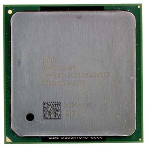 In due time we will get faster processors with FSB 800 MHz. But what is more important for most users who can't afford top-range processors is that lower-level models also equipped with the 800MHz bus are expected in May. Both this Pentium 4 3.0 GHz and other upcoming models will support Hyper-Threading which brings certain benefit (or loss) by making two logic processors out of one physical. In the whole line of Stepping D1 with multiple VID different processors can have different voltages in the range of 1.475 to 1.525 V (for those based on 0.13 micron technology), and heat dissipation of this particular Pentium 4 3GHz makes 81.9 W. This is noticeably more than the future lower models are going to have (under 70 W). 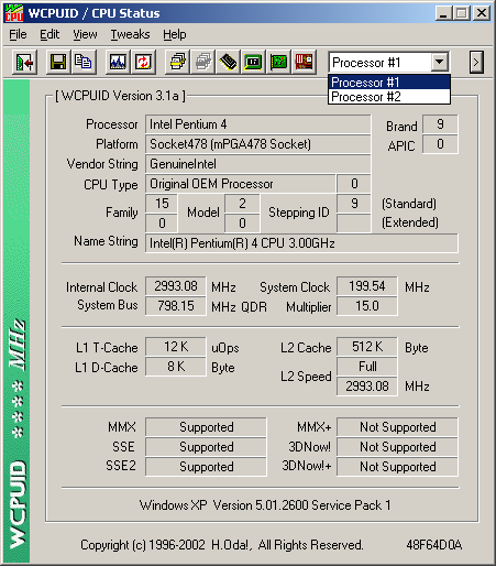 The 800MHz processors require new chipsets to run because currently there's no chipsets that officially support this FSB frequency (though overclockers can try to reach 200(800) MHz FSB with their old boards, and you will see an example below). But even an overclocked system will be just partly balanced, because most chipsets before the epoch of FSB 800 MHz supported only single-channel DDR memory, while the speediest DDR400 had only 3.2 GB/s. The bandwidth of the 800MHz bus of the new Pentium 4 is twice higher (6.4 GB/s), and there are other devices which need this band. Logically, new chipsets from Intel and other companies will support dual-channel DDR memory which doubles this figure (up to 6.4 GB/s with DDR400 used). Today we will test one of such chipsets. Intel 875P aka CanterwoodBy analogy with last year's line which supported FSB 533 MHz, i875P is the most efficient model in the expected series. On the other hand, this chipset doesn't have principal architectural differences from upcoming Springdales. Take a look at the chipset's diagram: 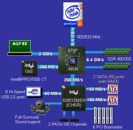 Numerous new features certainly need to be described. Since i875P is positioned as a substitute for i850E, i.e. as a high-performance solution, it supports only 533/800 MHz FBS (Willamette based processors do not support the new chipsets anyway). i875P works with DDR333 or DDR400 memory in the dual-channel mode; the latter memory type is supported only by processors equipped with the 800MHz bus. But system can actually work with FSB 400 MHz with DDR266 memory. By the way, the combination of 800/333 will force the memory work at 160(320) MHz - Intel says that it improves the sync modes, and therefore, boosts performance. The memory controller has conventional functions (for example, like that of iE7205); it utilizes the dual-channel mode with 2 (or 4 in pairs) memory modules of the same size and chip organization, and symmetrical contents of slots relating to different channels.  The chipset, being a desktop hi-end solution, supports memory with ECC enabled. Besides, it features the Intel PAT (Performance Acceleration Technology) to make up for the delay caused by error correction. It accelerates a data flow through MCH (unnecessary in this case sync buffers inside the chipset are not used, data are transferred directly) at 800/400 (FSB/memory). When the frequencies coincide the syncronization is minimal, and the fast silicon (with higher signal speed) used in i875P allows to refuse unnecessary buffers while "normal" chipsets still need them. According to Intel, the benefit achieved (in comparison with similar chipsets aka Springdale) makes 2-5%. It's not much, but it's something (though only with the 800MHz bus and dual-channel access to DDR400). Besides, it doesn't require any drivers or fooling around in BIOS. Beside the support of the dual-channel memory controller, fastest FSB (for desktop CPUs), and AGP 8x the north bridge (MCH) of the Canterwood sports a CSA bus (Communications Streaming Architecture). This solution will ensure high-speed connection of various devices to system resources, as well as access with a guaranteed bandwidth of a dedicated channel. Today there is only one solution for this bus - Gigabit Ethernet Intel PRO/1000 CT chip (Kenai II CSA), and no information is available on such chips from other companies. Such an expensive chip will hardly attract many board makers, and the CSA might remain unneeded. It's obvious why the engineers had to make a dedicated bus for the 1Gbit network adapter (in fact, CSA was created for this task), which, at the same time, goes from the north bridge: it's because of the lack of throughput in the previous solutions. As you know, the maximum throughput of a PCI bus, which is used for data transfer in case if an external network card, is 133 MB/s (actually, it will be less if we account for service data). It can limit 1Gbit network adapters, especially because of other PCI devices. Besides, a data flow from the PCI bus must go through various "matching" processes at the level of interhub connection controllers (for Intel's chipsets) in both hubs. If a disc subsystem is active, the channel which transfers data from the network controller gets narrower, and even integrated Gigabit Ethernet chips get bounded since they are attached to the south bridge. That is why it's better to connect the network controller directly to the north bridge (closer to the memory) via the bus of excessive throughput of 266 MB/s. 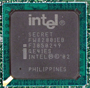
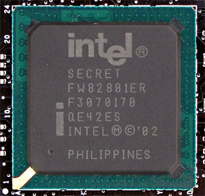 The south bridge also sports some new traits. Now it supports up to 8 USB (2.0) ports, and incorporates a Serial ATA controller supporting a RAID array (in ICH5R south bridge). Other features are standard: AC'97 v2.2 (up to 6 audio channels), 6 PCI 2.3 BusMaster devices, 2 [Parallel] ATA100 channels etc. VIA has announced a south bridge marked VT8237 with even a bit better characteristics, but its actual production will commence later. Now let's have a look at the integrated SATA controller. The good news is that no special drivers are needed for operation of SATA devices in any OSes. But in OSes not native for IDE (which do not support an arbitrary number of ATA controllers and need IRQ14 and IRQ15 for two logic IDE channels - all Microsoft's OSes except Windows 2000/XP) only the compatibility mode can be used. In this mode two IDE channels (a maximum of 4 devices) disable either one of PATA channels or both SATA ports, that is why devices connected to them won't be seen. In case of Windows XP (Windows 2000 is still studied) the ICH5R south bridge allows for a RAID0 array but only on two hard drives connected via SATA ports. Besides, Intel Application Accelerator RAID Edition initiates the process of creation of a RAID array in the background mode after the second hard drive is connected (with the OS installed on the first one) It doesn't need OS reinstallation and flows almost unnoticeably for a user. It's still studied whether RAID1 can be realized. If the outcome is positive, you will need just to update the software, like in case of technology certification for Windows 2000. Unfortunately, we didn't have enough Serial ATA hard drives at the time of writing this review, and we couldn't test this component of the south bridge. Finally, Intel's new line of chipsets needs only a 4-layer PCB design. It lowers the costs for mainboard production in comparison with the first desktop dual-channel Intel E7205. It was achieved at the expense of some optimizations in outputs and in MCH (the MCH chip turned at 45°, auto control of DRAM channels frequency syncronization, terminating resistors on die etc.). PerformanceTestbed:
Software:
Here are brief characteristics of the boards tested today for the first time:
ConclusionThe i875P chipset has some unique features like support of the integrated Serial ATA controller or even SATA RAID, of new Pentium 4's FSB and a dual-channel memory controller. It will be a good purchase for those who earlier wanted i850E or iE7205. This chipset provides all possible support, and the only downside is a lack of FireWire ports. PCs based on such chipset are not going to be too expensive. If you compare its performance with the maximum scores of Intel's chipsets of the previous generation, the benefit will make 5-20%. But most readers are not interested in the overclocking results, and in comparison with i845PE+DDR333 (+CPU on 533MHz FSB) the gain i875P achieves is 10-35% (it refers to all applications which markedly depend on memory). Although it may be incorrect to compare mainstream and top-performance chipsets, all functions and speed characteristics of Canterwood will hardly differ from the Springdale series, and we can judge about performance of the May's line by the i875P. Besides, the new chipset has nothing which would send priced of finished systems up, and I hope to see i875P based systems with a rational price tags (though they won't be too low due to a great number of integrated features). As to the gain from combining the Pentium 4 with the faster bus, it's
for you to decide whether it's much or little. Do remember that the speed
rises also at the expense of the chipsets. Some will be satisfied with
fps and seconds reached; others will be disappointed in the architecture
or some CPU makers because the performance does not double (at the expense
of the dual-channel memory) or at least rise 1.5 times (at the expense
of the bus); some others will be waiting for new chipsets and boards (instead
of the processors) which will bring richer functions at lower prices... As
new solutions will arrive in our lab, we will give you all ins and outs.
Write a comment below. No registration needed!
|
Platform · Video · Multimedia · Mobile · Other || About us & Privacy policy · Twitter · Facebook Copyright © Byrds Research & Publishing, Ltd., 1997–2011. All rights reserved. | |||||||||||||||||||||||||||||||||||||||||||||||||||||||||||||||||||||||||||||||||||||||||||||||||||||||||||||||||||||||||||||||||||||||||||||||||||||||||||||||||||||||||||||||||||||||||||||||||||||||||||||||||||||||||||||||||