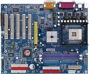
Jetway 845EDAK (i845E) Mainboard
|

Traditionally, we have received the board of this company in the OEM package.
But only a box is lacking. The board looks ordinary - a blue PCB and purple
memory slots.
Accessories:
-
Documentation: user manual in English;
-
Cables: 2 ATA66/100/133 and FDD;
-
Bracket for the rear computer panel;
-
Diskette with drivers for an additional IDE controller;
-
CD containing:
-
drivers;
-
Adobe Acrobat Reader;
-
Hardware Doctor;
-
PC-Cillin 2002;
-
Recovery Genius;
-
Magic BIOS;
-
Award Winflash;
-
DirectX 7.0 è 8.1.

The layout has several typical flaws: additional IDE connectors and
audio-ins are not in very good positions, and when a video card is installed
it's difficult to handle memory modules. It's not difficult to reach jumpers
when the board is already installed. Their functions are shown on the textolite.
The 3-channel switching voltage regulator incorporates 6 capacitors
of 3300 uF and 4 of 1200 uF.
The following controllers are integrated:
-
audio controller based on the ALC650 AC'97 codec supporting 5.1 audio systems
and having a connector for front audio inputs/outputs;
-
Additional IDE controller based on the Promise PDC20275 chip and supporting
up to 4 IDE devices via the ATA133 protocol.
The board supports the Recovery Genius technology for backup storing of
important data on HDD.
Non-unsoldered connectors: none.
The system monitoring is supported by the Winbond W83627HF-AW chip.
What is controlled:
-
voltage of processor, AGP bus, memory, +1.25, +3.3, +5 and +12 V, VBAT
and +5 V Standby;
-
speed of 3 fans;
-
temperatures of the processor (a built-in sensor), the board (a built-in
sensor) and an external sensor connected to the board.
There are 2 connectors for adjustable and 1 for unadjustable connection
of fans.
Brief characteristics of the board: memory slots - 2 DDR SDRAM;
expansion slots - AGP/ 5 PCI/ CNR; I/O ports - 2 COM/ LPT/ 2 PS/2/ 6 USB
2.0; dimensions - 305x245 mm.
Adjustment can be carried out with:
| jumpers and switches |
Jumper to clear up the CMOS |
|
| Jumpers to choose a FSB frequency |
Auto, 100 and 133 MHz |
| BIOS based on the AWARDBIOS 6.00PG from Phoenix |
Setup of memory timings |
+ |
CAS Latency, Cycle Time, RAS to CAS Delay, RAS Precharge |
| Setup of memory frequency |
+ |
Auto, DDR200, DDR266 |
| Setup of AGP bus |
+ |
|
| Setup of PCI bus |
- |
|
| Changeable scaler of AGP and PCI buses |
+ |
PCI (AGP/2) = FSB/3, FSB/4, FSB/5, FSB/6 |
| Manual assignment of interrupts |
- |
|
| Changeable FSB frequency |
+ |
100-200 MHz in 1MHz steps |
| Changeable CPU multiplier |
+ |
x8-x50 |
| Changeable core voltage |
+ |
1.1-1.85 V in 0.025V steps |
| Changeable memory voltage |
+ |
2.5, 2.6, 2.7, 2.8 V |
| Changeable chipset voltage |
- |
|
| Changeable AGP bus voltage |
+ |
1.5, 1.6 V |
We used the latest available version of the BIOS - A04.
This is board demonstrates an average performance; it combines a moderate
price and quite good overclocking tools.
Test results:
Write a comment below. No registration needed!
|
|
 |
|
|
|

