The today's comparison holds on to the typical tests of this kind carried
out in our lab. A top processor of one manufacturer is compared with that
of another, and they are coupled with the fastest for them chipsets. Apart
from the new processors the chipsets are also of great interest.
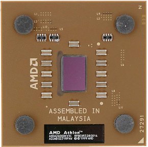
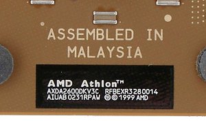
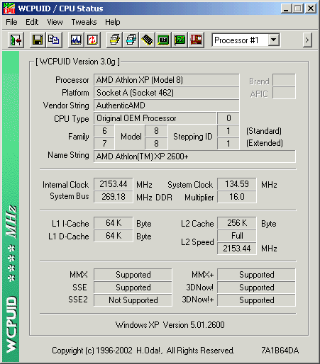
Athlon XP 2600+ processor
Although the lately released Athlon XP 2200+ and the latest Athlon XP
2400+/2600+ are based on a bit different Thoroughbred cores. The previous
core revision used in the 2200+ had the Stepping 0, and turned to be a
little raw, that is why the frequency couldn't be lifted over 1800 MHz.
Therefore, the redesigning of the Thoroughbred which brought us the stepping
1 is a forced step made to reach just the planned capabilities instead
of new summits. This case reminds me of the VIA Apollo KT266A, whose elder
brother KT266 came with a memory controller that couldn't provide the potential
stated in the specs.
The core of the new stepping has a greater surface (did they try to
eliminate problems of heat removal from a small surface?), a greater number
of transistors (by 400,000) and the maximum consumed power. AMD has changed
a policy of ratings. The 2400+ had actually to be clocked at 1800+2*66=1933
MHz ( 2000 MHz in fact), and the 2600+ at 1933+2*66=2066 MHz (2133 MHz
in fact). But it's known that at the fixed FSB frequency the performance
gain gets smaller as the multiplier (i.e. the core's frequency) grows up.
AMD proves that it takes very seriously its rating as an indicator of processor's
performance, and is not going to turn it into a meaningless figure.
The rumor has it that soon the Thoroughbred of Stepping 0 will be taken
out of production, and even the lowest model based on this core (2000+)
will be coupled with the Stepping 1. Well, taking into account the more
reliable core of the new stepping, this step of VIA is obvious, as the
KT266 was also gotten rid of when the KT266A appeared. :)
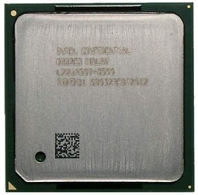
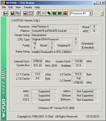
Intel Pentium 4 2.8 GHz processor
Actually, this is the Northwood itself as it uses a 0.13-micron process,
512 KB L2 cache, the FSB's speed is identical to 533 MHz in its bandwidth
(Quad Pumped Bus 133x4). This core lacks for an official support of the
Hyper-Threading technology, though the Northwood has it unofficially... :)
In the Pentium 4 2.8 GHz it's only the performance that will make interest
for us as it has nothing more to boast of as compared with the P4 2.53
GHz.
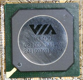
VIA Apollo KT400 chipset
There is a good principle: one should speak (write) about something
as much as a given thing is worth of. We will describe the new chipset
from VIA Technologies given to three aspects:
1. Those who want to keep abreast of all latest solutions of
the computer market have already downloaded all available information from
the VIA's site. Such readers may omit this section as they will hardly
find anything new here.
2. Those who prefer getting news from our site have probably read about the
VIA Apollo KT333, and in this
case they can read just about the differences between the KT400 and KT333.
3. Those who are not very interested in such things as support of certain
specs and memory types, frequencies and bandwidths of internal buses and
other highly specialized information on the KT333 chipset will hardly read
this section as well :).

So, what's the difference between the KT400 and KT333? Strange though
it may seem but we failed to find any official information that it supports
DDR of the same frequency as shown in the chipset's name. On the other
hand, this is a normal situation when the standard is not officially confirmed
by JEDEC and no one is sure it will be. But I think that the support of
the respective memory bus speed and even necessary divisors to make normal
PCI and AGP frequencies is provided in the KT400. But it's just an assumption
as the official information is lacking. But if it's true the BIOS of most
boards will let us enable the unsupported DDR 200 MHz, even without increasing
frequencies of other buses, as, for example, it was possible on the ASUS's
solution included into our test stand. :)
Another important innovation is a new 8X V-Link bus between the north
and south bridges providing 533 MB/s. Many expected the 8X V-Link yet in
the KT333, but it seems that VIA decided to combine two "8X" in one chipset
:). VIA Technologies thus caught up with Intel (the latest chips of this
company also use a bus in the chipset of the same throughput), and both
are behind SiS with its 1.2 GB/s MuTIOL developed a long time ago and boasting
of its fastest bus in the whole x86 kingdom. :)
The second "8X" is 8X AGP (AGP 3.0). Video cards and video chips supporting
this mode are already coming onto the scene, and soon they will let us
estimate its efficiency. However, nobody expects wonders: we just don't
want new bugs. By the way, VIA works excellently in this respect - it has
its won program of certification of AGP8X compatible 3D accelerators.
Other innovations are related with the south bridge, and they are quite
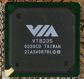
obvious: ATA133 was yet in the VT8233A south bridge; the current VT8235
also supports the USB 2.0.
The attention of experts can also be drawn by the "Future Pin Compatible
Upgrades with Serial-ATA and 802.11b", i.e. future south bridges supporting
these functions will be entirely pin compatible with the current VT8235
(and the whole line starting from the VT8233), which must cut expenses
for redesigning of the boards.
I must admit that the chipset is quite modern; it's the best choice
for today for Socket A based computers.
It should also be noted that the hypothesis of the 166 (333)
MHz FSB supported in the KT400 is not proven yet. Like in case of the DDR400
SDRAM, probably the FSB333 IS supported in this chipset. But we will make
it clear only when such processors become available.
Write a comment below. No registration needed!

