 |
||
|
||
| ||
|
||
|
||
| ||
We proceed with the analysis of the most important characteristics of high-performance DDR2 memory modules using our RightMark Memory Analyzer. Today we are going to review high-speed solutions from OCZ — three dual-channel 2-GB memory kits, Titanium and SLI-Ready series, PC2-6400, PC2-7200 and PC2-8000:
Manufacturer InformationModule manufacturer: OCZ Technology ExteriorOCZ DDR2 PC2-6400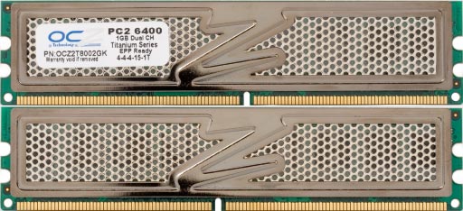 OCZ DDR2 PC2-7200 OCZ DDR2 PC2-8000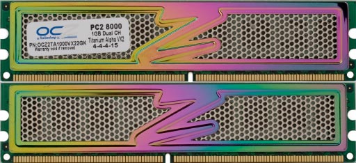 Part NumberThe manufacturer's web site does not publish the DDR2 Part Number expansion (we found out just an outdated manual about DDR memory modules). So we'll confine ourselves to a brief description of the modules, published on corresponding product web pages. OCZ DDR2 PC2-6400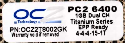 The new OCZ DDR2 PC2-6400 Titanium EPP-Ready modules are equipped with Enhanced Performance Profiles (EPP) to optimize the modules' performance on current nForce® 590 SLI-based motherboards. EPP profiles are programmed to boot at 800MHz DDR2 with supremely fast timings of 4-4-4 1T, that is the modules are capable of accepting one command per clock cycle (1T) so that memory performance is increased by a considerable amount. Each module comes equipped with integrated titanium-mirrored XTC (Xtreme Thermal Convection) heatspreaders for the most efficient heat dissipation. OCZ DDR2 PC2-7200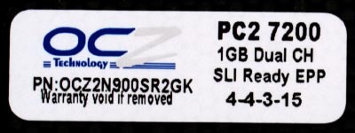 OCZ DDR2 PC2-7200 SLI-Ready Edition modules also support EPP. They are programmed to boot at DDR2-900 with 4-4-3 timings. According to the manufacturer, these modules come equipped with exclusive NVIDIA XTC heatspreaders for the most efficient heat dissipation and a look that stands out like its performance. OCZ DDR2 PC2-8000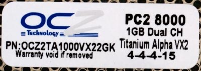 Unlike the first two representatives, OCZ DDR2 PC2-8000 Titanium Alpha VX2 modules lack EPP support. These modules belong to the proprietary Voltage Xtreme family, designed to operate at a high voltage (to obtain higher speed than available at the usual voltage level). This model is designed for DDR2-1000 and 4-4-4 timings owing to the raised voltage of 2.3V. It's positioned as a high-end solution for hardcore gamers and overclockers. Titanium-mirrored scratch-resistant XTC heatspreaders are also an exclusive solution, this time — with their colors (see the photo). Each Titanium Alpha module has a unique color and changes its hue depending on lighting and angle of view. SPD chip dataDescription of the general SPD standard:
Description of the specific SPD standard for DDR2:
EPP Standard Description:
OCZ DDR2 PC2-6400
According to SPD, supported CAS# latencies are 5, 4, and 3. The first value (CL X = 5) corresponds to the cycle time of 2.5 ns (400 MHz), i.e. DDR2-800. Not all timings for this case are integer. This scheme can be written as 5-5-5-14.8. Considering the most probable rounding up, it corresponds to the standard 5-5-5-15 timings. Reduced CAS# latency (CL X-1 = 4) corresponds to DDR2-667 (3.0 ns cycle time, 333.3 MHz) with noninteger 4-4.17-4.17-12.33 timings, which can be rounded up to 4-5-5-13. And finally, CAS# latency reduced by two (CL X-2 = 3) corresponds to slightly wrong but wide-spread DDR2-533 mode at the 3.7 ns cycle time (270.3 MHz) instead of nominal 3.75 ns (266.7 MHz). Timings for this case look like 3-3.37-3.37-10, rounded up to 3-4-4-10. Manufacturer's JEDEC ID Code, manufacturing date, and Part Number of the module are correct. But there is no information about its serial number. Besides, we don't like the looks of the strange SPD Revision 23h, which formally corresponds to nonexistent Revision 2.3. As these modules support EPP, let's analyze information from this "non-standard" part of SPD, represented by SPD Bytes 99-127.
EPP data are presented in the form of abbreviated profiles. There can be maximum four of them, while there is actually information only about the first profile (Profile 0), which is naturally marked as optimal. This abbreviated profile contains scarce information, which is published in the above table completely. The data include memory voltage — 2.0 V, address command rate (1T), cycle time (2.5 ns, 400 MHz memory bus, DDR2-800), and standard timings (4-4-4-14.8, rounded up to 4-4-4-15). The abbreviated EPP lacks additional parameters to fine-tune timings and electrical characteristics of memory. In our opinion, it discredits its main advantages. The manufacturer probably didn't pay proper attention to tweaking these characteristics. We'll see the consequences below, in the course of our module analysis. As for now, let's proceed to SPD of the next representative. OCZ DDR2 PC2-7200
Supported CAS# latencies — 5, 4, and 3. But cycle times are specified only for the first two values: main (CL X = 5) and reduced (CL X-1 = 4). The first value (CL X = 5) corresponds to the cycle time of 2.5 ns (400 MHz), i.e. DDR2-800. Timings for this case can be written with noninteger values as 5-5-5-14.8. They will be most likely rounded up to 5-5-5-15. The second value (CL X-1 = 4) corresponds to the slightly outdated DDR2-533 mode (3.75 ns cycle time, 266.7 MHz) with noninteger 4-3.33-3.33-9.87 timings, which can be rounded up to 4-4-4-10. As we have already noted above, CAS# latency reduced by two (CL X-2 = 3) does not correspond to any sensible operating mode, which is definitely a mistake. Manufacturer's JEDEC ID Code and Part Number of the module are correct. But there is no information about its manufacturing date and serial number. These modules also support EPP, so let's analyze information from this part of SPD.
EPP data look very interesting. Unlike the above OCZ DDR2 PC2-6400 modules with abbreviated EPP profiles, the OCZ DDR2 PC2-7200 modules contain information about two full profiles (Profiles 0 and 1). Both of them are valid, but they correspond... to almost identical operating modes(!), there are only minor differences. Namely, both profiles set memory modules to DDR2-900 (approximately 454.5 MHz, 2.2 ns cycle time) at 2.3 V (complies with manufacturer's specifications) and 2T address command rate. Only main memory timings differ a little. In the first case they look like 4-3.98-2.84-15 (rounded up to 4-4-3-15). The second case - 4-3.75-2.84-14.09. When rounded up, we also get 4-4-3-15 (matches the official scheme), but EPP profiles also differ in other timings like tWR and tRC. Anyway, Profile 1 is considered optimal. SPD data in the OCZ DDR2 PC2-7200 modules (including the EPP extensions) evidently differ from SPD (and EPP) data in the OCZ DDR2 PC2-6400 modules reviewed above. This way or another, there are some inaccuracies or even mistakes in both cases. Thus, OCZ's approach to programming SPD is quite original, if not slipshod. In conclusion let's examine SPD in our last contender — OCZ DDR2 PC2-8000. These modules do not support EPP, so SPD contains only the "standard" section. OCZ DDR2 PC2-8000
SPD data in these modules are similar to those in the first product we reviewed today — OCZ DDR2 PC2-6400. Supported CAS# latencies are 5, 4, and 3. The first value (CL X = 5) corresponds to the cycle time of 2.5 ns (400 MHz), i.e. DDR2-800. Timings for this case are written as 5-5-5-14.8 (5-5-5-15). Reduced CAS# latency (CL X-1 = 4) corresponds to DDR2-667 (3.0 ns cycle time, 333.3 MHz) with 4-4.17-4.17-12.33 (4-5-5-13) timings. And finally, CAS# latency reduced by two (CL X-2 = 3) corresponds to erroneous but wide-spread DDR2-533 with the cycle time of 3.7 ns (270.3 MHz). Timings for this case are written as 3-3.37-3.37-10.0 (3-4-4-10). Manufacturer's JEDEC ID Code and Part Number of the modules are correct; but there is no information about their manufacturing date and serial numbers. Testbed configurationTestbed 1
Test resultsThe OCZ modules were tested on the AMD platform (Athlon 64 X2 4800+) based on the ASUS CROSSHAIR motherboard (Testbed 1) that supports EPP. The modules were tested in two modes in all cases: 1. Nominal: standard CPU frequency, 400 MHz memory (DDR2-800), standard memory settings (by SPD), EPP data are not used. 2. Optimal, corresponds to the optimal EPP profile, allows to overclock a processor (up to 15%) to get maximum recommended memory frequency. We configured CPU and memory frequencies manually in case of OCZ DDR2 PC2-8000 modules, which do not support EPP. OCZ DDR2 PC2-6400
Let's start with test results of OCZ DDR2 PC2-6400 memory modules. They officially support DDR2-800 mode with 4-4-4-15 timings, and most importantly, 1T address command rate. As you can see on the table above, BIOS sets memory timings for these modules to 5-5-5-15-2T by default. Their performance is on the typical DDR2-800 level for this CPU frequency (2.4 GHz). Memory voltage raised to 2.2 V, timings can be reduced to 4-4-3 (like most other DDR2 models, these modules are not sensitive to changes of the last standard timing - tRAS), but the address command rate must still be 2T. Attempts to use hardcore timings 4-3-3-2T as well as 1T mode with any timings resulted in memory system errors. Thus, OCZ DDR2 PC2-6400, modules, designed for DDR2-800 4-4-4-15-1T, cannot operate in this mode. The EPP profile failed to save the day (no wonder, EPP data in these modules are represented by a single abbreviated profile, which does not allow to tweak additional timings and voltages), even when we tried to raise voltage to 2.3 V. OCZ DDR2 PC2-7200
When the OCZ DDR2 PC2-7200 modules operated in the standard DDR2-800 mode, our ASUS CROSSHAIR motherboard set timings to 5-5-5-15-2T (like in the previous case). Performance of PC2-7200 modules in this mode is similar to that of PC2-6400 modules reviewed above. But the most interesting fact is that when memory voltage is raised (to 2.3 V), these modules can set 4-4-3 timings at the 1T address command rate. That's their biggest difference from the PC2-6400 modules reviewed above, which officially(!) work in 1T mode. Moreover, we managed to run these modules with 3-3-3-1T timings, but they resulted in errors. The optimal EPP profile sets FSB clock to 228 MHz, which corresponds to 228x2 = 456 MHz memory bus frequency ("DDR2-912", a tad higher than the nominal "DDR2-900" mode) with 2.74 GHz CPU clock (CPU voltage was manually increased to 1.5 V for the sake of stability). In this case the timings were set to 4-4-3-15-2T, matching the manufacturer's scheme. The memory modules under review can still operate in this mode, but further reduction of timings (except for the ignored tRAS) as well as of the address command rate to 1T resulted in memory instability. OCZ DDR2 PC2-8000
When we used OCZ DDR2 PC2-8000 modules in the official DDR2-800 mode, the ASUS CROSSHAIR motherboard set 5-5-5-15-2T timings by default. As in case with PC2-7200 modules (not PC2-6400), raising memory voltage to 2.3 V allows to reduce timings to 4-3-3 (further reduction to 3-3-3 results in errors) and address command rate to 1T. Performance results of PC2-8000 and PC2-7200 modules are practically identical in this case. As the OCZ DDR2 PC2-8000 modules do not support EPP, we set the "DDR2-1000" mode manually by increasing the system bus frequency to 250 MHz to get 500 MHz memory and 2.5 GHz CPU (250x10). Minimal timings under these conditions are 4-4-4-2T at 2.3 V. This result matches the official values (an attempt to set lower timings immediately resulted in memory failures). Bottom lineTested samples of high-speed memory modules from OCZ (PC2-6400, PC2-7200, and PC2-8000) produce an ambiguous impression. The most unpleasant impression is produced by the careless approach of the manufacturer to programming SPD data (EPP in particular), which can have an immediate effect on compatibility of memory modules with various motherboards. Moreover, the first of the samples reviewed (PC2-6400) couldn't operate in the standard officially supported mode at 1T address command rate (at least on the ASUS CROSSHAIR motherboard). What concerns goodies, the other two representatives (PC2-7200 SLI-Ready Edition and PC2-8000 Titanium Alpha VX2) can operate in the standard DDR2-800 mode with "extreme" 4-3-3 timings and 1T address command rate. This is not quite typical of most 2 GB dual-channel memory kits for AMD AM2. At the same time, memory modules of these series seem to be overclocked to the limit in unofficial modes ("DDR2-900" and "DDR2-1000", correspondingly), because it's impossible to reduce timings as well as the address command rate (to 1T) any further. But stable operation of PC2-7200/PC2-8000 modules in the fastest modes is an advantage of these OCZ series, considering the problem with PC2-6400 modules.
Write a comment below. No registration needed!
|
Platform · Video · Multimedia · Mobile · Other || About us & Privacy policy · Twitter · Facebook Copyright © Byrds Research & Publishing, Ltd., 1997–2011. All rights reserved. | ||||||||||||||||||||||||||||||||||||||||||||||||||||||||||||||||||||||||||||||||||||||||||||||||||||||||||||||||||||||||||||||||||||||||||||||||||||||||||||||||||||||||||||||||||||||||||||||||||||||||||||||||||||||||||||||||||||||||||||||||||||||||||||||||||||||||||||||||||||||||||||||||||||||||||||||||||||||||||||||||||||||||||||||||||||||||||||||||||||||||||||||||||||||||||||||||||||||||||||||||||||||||||||||||||||||||||||||||||||||||||||||||||||||||||||||||||||||||||||||||||||||||||||||||||||||||||||||||||||||||||||||||||||||||||||||||||||||||||||||||||||||||||||||||||||||||||||||||||||||||||||||||||||||||||||||||||||||||||||||||||||||||||||||||||||||||||||||||||||||||||||||||||||||||||||||||||||||||||||||||||||||||||


