DDR Memory Module Analysis. Part 6: G.Skill DDR-500 Modules
|
We proceed with the series of articles, dedicated to the low level analysis of the most important characteristics of DDR memory modules using our RightMark Memory Analyzer test package. Today is the second time when we are going to review DDR memory modules of large capacity — a couple of high-speed G.Skill DDR-500 modules with the total capacity of 2 GB.
Manufacturer Information
Module manufacturer: G.Skill
Manufacturer of module chips: unknown
Web site of the module manufacturer: http://www.gskill.com/ddr.html
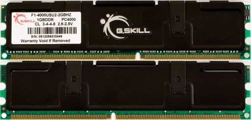
Module Exterior
Photo of the memory module
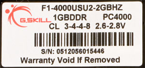
Module Part Number
The manufacturer's web site does not publish the DDR Part Number expansion. Brief description of these modules on the official web site specifies that this product is a matched pair of memory modules of the uncertified DDR-500 standard (PC4000). They are the first modules of the HZ series with the total capacity of 2 GB (hence, capacity of a single module is 1 GB). In this mode, the modules can operate with 3-4-4-8 timings at a relatively low voltage of 2.6-2.8 V.
SPD chip data
Description of the general SPD standard:
JEDEC Standard No. 21-C, 4.1.2 - SERIAL PRESENCE DETECT STANDARD, General Standard
Description of the specific SPD standard for DDR:
JEDEC
Standard No. 21-C, 4.1.2.4 — Appendix D, Rev. 1.0: SPD’s
for DDR SDRAM
| Parameter |
Bytes |
Value |
Expansion |
| Fundamental Memory Type |
2 |
07h |
DDR SDRAM |
| Number of Row Addresses on this assembly |
3 |
0Dh |
13 (RA0-RA12) |
| Number of Column Addresses on this assembly |
4 |
0Bh |
11 (CA0-CA10) |
| Number of DIMM Banks |
5 |
02h |
2 physical banks |
| Data Width of this assembly |
6, 7 |
40h, 00h |
64 bit |
| Voltage Interface Level of this assembly |
8 |
04h |
SSTL 2.5V |
| SDRAM Cycle time (tCK) at maximum supported CAS# latency (CL X) |
9 |
50h |
4.0 ns (250.0 MHz) |
| DIMM configuration type |
11 |
00h |
Non-ECC |
| Refresh Rate/Type |
12 |
82h |
7.8125 ms — 0.5x reduced self-refresh |
| Primary SDRAM Width (organization type) of the memory module chips |
13 |
08h |
x8 |
| Error Checking SDRAM Width (organization type) of the memory chips in the ECC module |
14 |
00h |
Not defined |
| Burst Lengths Supported (BL) |
16 |
0Eh |
BL = 2, 4, 8 |
| Number of Banks on SDRAM Device |
17 |
04h |
4 |
| CAS Latency (CL) |
18 |
10h |
CL = 3.0 |
| Minimum clock cycle (tCK) at reduced CAS# latency (CL X-0.5) |
23 |
00h |
Not defined |
| Minimum clock cycle (tCK) at reduced CAS# latency (CL X-1.0) |
25 |
00h |
Not defined |
| Minimum Row Precharge Time (tRP) |
27 |
3Ch |
15.0 ns
3.75 (4), CL = 3.0 |
| Minimum Row Active to Row Active delay (tRRD) |
28 |
28h |
10.0 ns
2.5, CL = 3.0 |
| Minimum RAS to CAS delay (tRCD) |
29 |
3Ch |
15.0 ns
3.75 (4), CL = 3.0 |
| Minimum Active to Precharge Time (tRAS) |
30 |
20h |
32.0 ns
8, CL = 3.0 |
| Module Bank Density |
31 |
80h |
512 MB |
| SDRAM Device Minimum Active to Active/Auto Refresh Time (tRC) |
41 |
00h |
Not defined |
| SDRAM Device Minimum Auto-Refresh to Active/Auto-Refresh Command Period (tRFC) |
42 |
00h |
Not defined |
| Maximum device cycle time (tCKmax) |
43 |
00h |
Not defined |
| SPD Revision |
62 |
01h |
Revision 0.1 |
| Checksum for Bytes 0-62 |
63 |
AEh |
174 (true) |
| Manufacturer’s JEDEC ID Code (only the first significant bytes are shown) |
64-71 |
7Fh, 7Fh,
7Fh, 7Fh,
CDh |
Corsair |
| Module Part Number |
73-90 |
— |
HZ |
| Module Manufacturing Date |
93-94 |
00h, 00h |
Not defined |
| Module Serial Number |
95-98 |
00h, 00h,
00h, 00h |
Not defined |
SPD contents do not look standard (not surprising, considering that these modules are not standard themselves). Only one CAS# latency is supported (CL X) = 3, which corresponds to the cycle time of 4.0 ns (operating in non-standard DDR-500 mode). The timing scheme corresponding to this only case looks somewhat strange, as it contains fractional tRCD and tRP — 3-3.75-3.75-8. Nevertheless, considering that most BIOS versions usually round up fractional values in memory settings, we get the 3-4-4-8 scheme, specified by the manufacturer. There is a shortcoming - no SPD information about timings for the standard DDR-400 mode, necessary for the system to set memory parameters correctly by default. This option should have been written for the reduced CAS# latency (CL X-0.5) — the proper scheme might have looked like 2.5-3-3-6.4 (rounded up to 2.5-3-3-7).
Among other SPD peculiarities we can mention undefined absolute values for tRC and tRFC and maximum device cycle time (tCKmax), as well as a strange SPD revision "0.1" and no data on manufacturing date and serial number. What concerns Part Number, you can see that the corresponding text field indicates HZ series, but it does not contain a specific number of these modules.
Testbed configuration and software
- CPU: AMD Athlon 64 4000+, 2.4 GHz (ClawHammer rev. SH-CG, 1 MB L2)
- Chipset: NVIDIA nForce4 SLI X16
- Motherboard: MSI K8N Diamond Plus, BIOS 080012 dated 12/22/2005
- Memory: 2x1024 MB G.Skill PC4000, DDR-500 (in DDR-400 mode)
- Video: Leadtek PX350 TDH, NVIDIA PCX5900
- HDD: WD Raptor WD360, SATA, 10000 rpm, 36Gb
- Drivers: NVIDIA Forceware 77.72, NVIDIA nForce4 X16 6.82, DirectX 9.0c
Test Results
Performance tests
The modules were tested in the standard mode — DDR-400. As usual, in the first series of tests memory timings were set by default (BIOS Setup — Memory Timings: "by SPD"). One of the motherboards, recommended by the module manufacturer and used in our tests, MSI K8N Diamond Plus, set its timings in this case to 3-3-3-7, which is somewhere between the official 3-4-4-8 scheme for DDR-500 and the proper DDR-400 scheme (mentioned above) — 2.5-3-3-7.
| Parameter |
G.Skill PC4000 |
Corsair XMS-3500LLPRO |
| Timings |
3-3-3-7
|
2-3-2-6
|
| Average memory read bandwidth,
MB/sec |
3916
|
4344
|
| Average memory write bandwidth,
MB/sec |
2409
|
2555
|
| Max. memory read bandwidth,
MB/sec |
6286
|
6400
|
| Max. memory write bandwidth,
MB/sec |
6016
|
6213
|
| Minimum Pseudo-Random
Access Latency, ns |
38.9
|
31.6
|
| Maximum Pseudo-Random
Access Latency, ns |
42.2
|
35.3
|
| Minimum Random Access
Latency*, ns |
72.7
|
62.8
|
| Maximum Random Access
Latency*, ns |
76.5
|
67.0
|
*16 MB block size
Speed characteristics of G.Skill modules look average (for comparison, the table contains the results of high-speed DDR modules Corsair XMS-3500LLPRO) — memory bandwidth is lower by about 100-200 MB/s, memory access latencies are higher by 7-10 ns compared to the modules specified.
Stability tests
Timing values, except for tCL, were adjusted "on the fly" due to the built-in RMMA feature that allows to change dynamically memory settings supported by the chipset (in this case - by the memory controller integrated into Athlon 64). Memory operating stability was evaluated with an auxiliary utility RightMark Memory Stability Test, included into RMMA.
| Parameter |
G.Skill PC4000 |
Corsair XMS-3500LLPRO |
| Timings |
2.5-3-3-5(-7-10)
|
2-3-2-5(-7-10)
|
| Average memory read bandwidth,
MB/sec |
3917
|
4355
|
| Average memory write bandwidth,
MB/sec |
2425
|
2572
|
| Max. memory read bandwidth,
MB/sec |
6298
|
6410
|
| Max. memory write bandwidth,
MB/sec |
6106
|
6211
|
| Minimum Pseudo-Random
Access Latency, ns |
37.7
|
31.5
|
| Maximum Pseudo-Random
Access Latency, ns |
41.1
|
35.3
|
| Minimum Random Access
Latency*, ns |
69.9
|
62.5
|
| Maximum Random Access
Latency*, ns |
73.6
|
66.7
|
*16 MB block size
The new 1 GB memory modules on MSI K8N Diamond Plus allowed quite unassuming minimum timings in DDR-400 mode without losing stability — 2.5-3-3-5. That is we managed to reduce CAS# latency to just 2.5 (the last value, tRAS, shouldn't be taken literally — as we know from our multiple reviews, most modules are indifferent to its changes).
The effect of overclocking timings is not high — we can notice some decrease in pseudo-random and random memory access latencies by about 1-3 ns.
Bottom line
G.Skill DDR-500 memory modules with the total capacity of 2 GB offer moderate performance characteristics and a moderate timings overclocking potential — minimal timings in DDR-400 mode are just 2.5-3-3-5. Considering that DDR modules of high capacity is a new trend — both for this manufacturer as well as for the industry on the whole, we can expect modules of this type with better characteristics in future.
Write a comment below. No registration needed!
|
|
 |
|
|
|