Memory Module Analysis. Part 12: GeIL DDR2-667 Modules
|
We proceed with the series of articles, dedicated to the low level analysis of the most important characteristics of DDR2 memory modules using our RightMark Memory Analyzer test package. In this article we are going to review a pair of 512MB DDR2-667 modules, manufactured by Golden Emperor International Ltd. (GeIL is an abbreviation).
Manufacturer Information
Module manufacturer: Golden Emperor International Ltd. (GeIL)
Manufacturer of module chips: Golden Emperor International Ltd. (GeIL)
Web site of the module manufacturer: http://www.geil.com.tw/portal/product.php
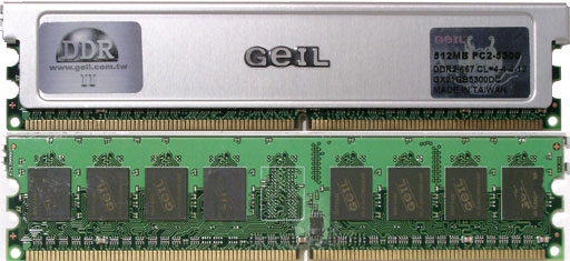
Module Appearance
Photo of the memory module

Module Part Number

There is no Part Number expansion on the product page (http://www.geil.com.tw/portal/product_DDR2-667DC.php). The manufacturer provides only brief module characteristics:
- Performance characteristics: PC5300 (PC2-5300 would be more correct), 667 MHz, 4-4-4 timings
- Chips: 64x8 DDR2 in FBGA-package
- Module parameters: 240-pin, non-ECC, unbuffered
- Aluminium heatsink
- 6-layered screened PCB with a very low interference level
- Voltage: 1.8 — 1.9V
SPD module chip data
Description of the general SPD standard:
Description of the specific SPD standard for DDR2:
| Parameter |
Byte |
Value |
Expansion |
| Fundamental Memory Type |
2 |
08h |
DDR2 SDRAM |
| Number of Row Addresses on this assembly |
3 |
0Eh |
14 (RA0-RA13) |
| Number of Column Addresses on this assembly |
4 |
0Ah |
10 (CA0-CA9) |
| Number of DIMM Banks |
5 |
60h |
1 physical bank |
| Data Width of this assembly |
6 |
40h |
64 bit |
| Voltage Interface Level of this assembly |
8 |
05h |
SSTL 1.8V |
| SDRAM Cycle time (tCK) at maximum supported CAS# latency (CL X) |
9 |
30h |
3.00 ns (333.3 MHz) |
| DIMM configuration type |
11 |
00h |
Non-ECC |
| Refresh Rate/Type |
12 |
82h |
7.8125 ms — 0.5x reduced self-refresh |
| Primary SDRAM Width (organization type) of the memory module chips |
13 |
08h |
x8 |
| Error Checking SDRAM Width (organization type) of the memory chips in the ECC module |
14 |
00h |
Not defined |
| Burst Lengths Supported (BL) |
16 |
0Ch |
BL = 4, 8 |
| Number of Banks on SDRAM Device |
17 |
04h |
4 |
| CAS Latency (CL) |
18 |
38h |
CL = 5, 4, 3 |
| Minimum clock cycle (tCK) at reduced CAS# latency (CL X-1) |
23 |
3Dh |
3.75 ns (266.7 MHz) |
| Minimum clock cycle (tCK) at reduced CAS# latency (CL X-2) |
25 |
50h |
5.00 ns (200.0 MHz) |
| Minimum Row Precharge Time (tRP) |
27 |
30h |
4, CL = 5
3 (3.2), CL = 4
2 (2.4), CL = 3 |
| Minimum Row Active to Row Active delay (tRRD) |
28 |
1Eh |
2.5, CL = 5
2.0, CL = 4
1.5, CL = 3 |
| Minimum RAS to CAS delay (tRCD) |
29 |
30h |
12.0 ns
4, CL = 5
3 (3.2), CL = 4
2 (2.4), CL = 3 |
| Minimum Active to Precharge Time (tRAS) |
30 |
2Dh |
45.0 ns
15, CL = 5
12, CL = 4
9, CL = 3 |
| Module Bank Density |
31 |
80h |
512 MB |
| Write recovery time (tWR) |
36 |
3Ch |
15.0 ns
5, CL = 5
4, CL = 4
3, CL = 3 |
| Internal write to read command delay (tWTR) |
37 |
1Eh |
7.5 ns
2.5, CL = 5
2.0, CL = 4
1.5, CL = 3 |
| Internal read to precharge command delay (tRTP) |
38 |
1Eh |
7.5 ns
2.5, CL = 5
2.0, CL = 4
1.5, CL = 3 |
| SDRAM Device Minimum Active to Active/Auto Refresh Time (tRC) |
41, 40 |
3Ch, 00h |
60.0 ns
20, CL = 5
16, CL = 4
12, CL = 3 |
| SDRAM Device Minimum Auto-Refresh to Active/Auto-Refresh Command Period (tRFC) |
42, 40 |
69h, 00h |
105.0 ns
35, CL = 5
28, CL = 4
21, CL = 3 |
| Maximum device cycle time (tCKmax) |
43 |
80h |
8.0 ns |
| SPD Revision |
62 |
10h |
Revision 1.0 |
| Checksum for Bytes 0-62 |
63 |
BCh |
188 (true) |
| Manufacturer’s JEDEC ID Code |
64-71 |
FFh, 7Fh,
7Fh, 13h |
Golden Empire |
| Module Part Number |
73-90 |
— |
GX21GB5300DC |
| Module Manufacturing Date |
93-94 |
FFh, FFh |
Not correct |
| Module Serial Number |
95-98 |
20h, 02h,
07h, 25h |
25070220h |
According to the SPD data, the reviewed modules can operate with three different CAS# latencies, each one corresponds to its own cycle time (working frequency). Thus, the maximum CAS# latency (5) corresponds to DDR2-667 mode (3.0 ns, 333.3 MHz), the reduced CAS# latency (4) — to the DDR2-533 mode (3.75 ns, 266.7 MHz), and finally the least CAS# latency (3) — to the DDR2-400 mode (5.0 ns, 200.0 MHz). Note that the absolute timings values tRCD and tRP are somewhat reduced (12 ns) relative to the typical (15 ns) values for DDR2 memory. It consequently has an effect on the relative values in timing schemes, which can be written as follows:
| Mode | Timings |
| DDR2-667 | 5-4-4-15 |
| DDR2-533 | 4-3-3-12 (rounded off to the nearest integer) |
| DDR2-400 | 3-2-2-9 (rounded off to the nearest integer) |
The timing scheme for DDR2-667 differs much from the 4-4-4(-12) scheme claimed on the module and on the description page, in a bad sense at that. The other schemes are obtained by rounding off tRCD and tRP to the nearest integer (in this case — they are rounded down). But the practice shows (we are going to see that again below) that almost all motherboards round the values up, when the memory system is configured automatically (to all appearances, on maximum stability grounds).
Among the other SPD peculiarities we can note a Part Number (which matches the one specified on the modules) and a serial number. You should also note that the module manufacturing date is not just absent but wrong. Testbed Configurations and Software
Testbed #1
- CPU: Intel Pentium 4 3.4 GHz (Prescott D0, 1 MB L2)
- Chipset: Intel 925X
- Motherboard: Gigabyte
8ANXP-D, BIOS F1 dated 06/07/2004
- Memory: 2x512 MB GeIL DDR2-667
- Video: Leadtek PX350 TDH, nVidia PCX5900
- HDD: WD Raptor WD360, SATA, 10000 rpm, 36Gb
- Drivers: nVidia Forceware 62.01, Intel Chipset Utility 6.0.1.1002, DirectX 9.0c
Testbed #2
- CPU: Intel Pentium 4 3.4 GHz (Prescott D0, 1 MB L2)
- Chipset: Intel 925X
- Motherboard: MSI 925X Neo,
BIOS dated 06/18/2004
- Memory: 2x512 MB GeIL DDR2-667
- Video: Leadtek PX350 TDH, nVidia PCX5900
- HDD: WD Raptor WD360, SATA, 10000 rpm, 36Gb
- Drivers: nVidia Forceware 62.01, Intel Chipset Utility 6.0.1.1002, DirectX 9.0c
Testbed #3
- CPU: Intel Pentium 4 3.4 GHz (Prescott D0, 1 MB L2)
- Chipset: Intel 915P
- Motherboard: MSI
915P Neo2, BIOS V1.3B0 dated 09/08/2004
- Memory: 2x512 MB GeIL DDR2-667
- Video: Leadtek PX350 TDH, nVidia PCX5900
- HDD: WD Raptor WD360, SATA, 10000 rpm, 36Gb
- Drivers: nVidia Forceware 62.01, Intel Chipset Utility 6.0.1.1002, DirectX 9.0c
Testbed #4
- CPU: Intel Pentium 4 3.4 GHz (Prescott D0, 1 MB L2)
- Chipset: Intel 915P
- Motherboard: ECS PF4 Extreme,
BIOS dated 06/01/2004
- Memory: 2x512 MB GeIL DDR2-667
- Video: Leadtek PX350 TDH, nVidia PCX5900
- HDD: WD Raptor WD360, SATA, 10000 rpm, 36Gb
- Drivers: nVidia Forceware 62.01, Intel Chipset Utility 6.0.1.1002, DirectX 9.0c
Testbed #5
- CPU: Intel Pentium 4 3.4 GHz (Prescott D0, 1 MB L2)
- Chipset: Intel 915G
- Motherboard: MSI 915G
Combo, BIOS 080011 dated 07/14/2004
- Memory: 2x512 MB GeIL DDR2-667
- Video: Leadtek PX350 TDH, nVidia PCX5900
- HDD: WD Raptor WD360, SATA, 10000 rpm, 36Gb
- Drivers: nVidia Forceware 62.01, Intel Chipset Utility 6.0.1.1002, DirectX 9.0c
Testbed #6
- CPU: Intel Pentium 4 3.6 GHz (Prescott E0, 1 MB L2)
- Chipset: Intel 925XE, 200 MHz FSB
- Motherboard: ECS PF21
Extreme, BIOS dated 12/07/2004
- Memory: 2x512 MB GeIL DDR2-667
- Video: Leadtek PX350 TDH, nVidia PCX5900
- HDD: WD Raptor WD360, SATA, 10000 rpm, 36Gb
- Drivers: nVidia Forceware 62.01, Intel Chipset Utility 6.0.1.1002, DirectX 9.0c
Testbed #7
- CPU: Intel Pentium 4 3.6 GHz (Prescott E0, 1 MB L2) at 3.73 GHz (266 MHz x14)
- Chipset: Intel 925XE, 266 MHz FSB
- Motherboard: ECS PF21
Extreme, BIOS dated 12/07/2004
- Memory: 2x512 MB GeIL DDR2-667
- Video: Leadtek PX350 TDH, nVidia PCX5900
- HDD: WD Raptor WD360, SATA, 10000 rpm, 36Gb
- Drivers: nVidia Forceware 62.01, Intel Chipset Utility 6.0.1.1002, DirectX 9.0c
Test Results
We tested GeIL DDR2-667 modules in the DDR2-533 mode, because (1) most motherboards in our tests (on i915P/G and i925X chipsets) do not support DDR2-667 mode at all; (2) it's useless in many respects, because the memory bandwidth is limited by the FSB throughput, which is 6.4 GB/sec at 200-MHz and 8.53 GB/sec at 266-MHz FSB. The peak DDR2-667 throughput in dual channel mode is 10.66 GB/sec. Performance tests
The first series of tests used the "standard" timing values, set by BIOS "by SPD". As we have already noted, most BIOS routines for configuring the memory system tend to round fractional figures up — which in this case resulted in the 4-4-4-12 scheme, regular for DDR2-533.
Note that the modules under review refused to work with ECS PF21 Extreme motherboard (Testbeds 6 and 7). Of course, the motherboard was configured for the 200 MHz and 266 MHz modes beforehand with other memory modules.
| Parameter |
Testbed 1 |
Testbed 2 |
Testbed 3 |
Testbed 4 |
Testbed 5 |
Testbed 6 |
Testbed 7* |
| Timings |
4-4-4-12 |
4-4-4-12 |
4-4-4-12 |
4-4-4-12 |
4-4-4-12 |
— |
— |
| Average memory read bandwidth, MB/sec |
4892
|
4943
|
4770
|
4769
|
4719
|
—
|
—
|
| Average memory write bandwidth, MB/sec |
2113
|
2017
|
2017
|
2031
|
2002
|
—
|
—
|
| Max. memory read bandwidth, MB/sec |
6435
|
6497
|
6436
|
6436
|
6371
|
—
|
—
|
| Max. memory write bandwidth, MB/sec |
4287
|
4327
|
4323
|
4309
|
4266
|
—
|
—
|
| Minimum Pseudo-Random Access Latency, ns
|
48.7
|
48.2
|
51.1
|
51.0
|
51.7
|
—
|
—
|
| Maximum Pseudo-Random Access Latency, ns |
56.0
|
55.4
|
58.3
|
58.3
|
59.0
|
—
|
—
|
| Minimum Random Access Latency**,
ns |
118.5
|
117.2
|
122.1
|
122.7
|
123.9
|
—
|
—
|
| Maximum Random Access Latency**,
ns |
137.7
|
136.0
|
140.9
|
141.3
|
142.7
|
—
|
—
|
*FSB frequency — 266.7 MHz
**16MB block size
The best memory system performance results (maximum memory bandwidth, minimum latency) were demonstrated by motherboards based on the i925X chipset — MSI 925X Neo (Testbed 2) and Gigabyte 8ANXP-D (Testbed 1). Motherboards on the i915P chipset — MSI 915P Neo2 (Testbed 3) and ECS PF4 Extreme (Testbed 4) are in between, and the last place is expectedly taken by the combo DDR/DDR2 solution MSI 915G Combo (Testbed 5) on the i915G chipset.
Stability tests
Timing values (except for tCL) were adjusted "on the fly" due to the built-in RMMA feature that allows to change dynamically memory settings supported by the chipset. Memory operation stability was evaluated in our specially developed utility, which will soon be released as a stand-alone application and will come shipped with RMMA.
The minimal timing values, which we managed to get from these modules on all motherboards, 3-3-2, can be considered quite good. Namely, we managed to reduce tCL by one, tRCD — to haul up to the nominal value claimed in the SPD (which is just a tad lower than the absolute record of 3-2-2, achieved by Corsair XMS2 PRO modules), and to reduce tRP by 2 cycles relative to the standard and by one relative to the nominal value. The last parameter (tRAS), in the chipset settings, is ignored by these memory modules as well as by the majority of other DDR2 modules.
| Parameter |
Testbed 1 |
Testbed 2 |
Testbed 3 |
Testbed 4 |
Testbed 5 |
Testbed 6 |
Testbed 7* |
| Timings |
3-3-2
|
3-3-2
|
3-3-2
|
3-3-2
|
3-3-2
|
—
|
—
|
| Average memory read bandwidth, MB/sec |
5143
|
5191
|
5002
|
4990
|
4931
|
—
|
—
|
| Average memory write bandwidth, MB/sec |
2302
|
2320
|
2228
|
2248
|
2252
|
—
|
—
|
| Max. memory read bandwidth, MB/sec |
6509
|
6567
|
6538
|
6519
|
6460
|
—
|
—
|
| Max. memory write bandwidth, MB/sec |
4287
|
4331
|
4323
|
4309
|
4266
|
—
|
—
|
| Minimum Pseudo-Random Access Latency, ns
|
46.6
|
46.2
|
48.5
|
48.8
|
49.3
|
—
|
—
|
| Maximum Pseudo-Random Access Latency, ns |
53.6
|
53.2
|
56.0
|
56.1
|
56.9
|
—
|
—
|
| Minimum Random Access Latency**,
ns |
103.4
|
102.8
|
107.9
|
108.3
|
109.2
|
—
|
—
|
| Maximum Random Access Latency**,
ns |
124.3
|
123.4
|
128.0
|
128.4
|
129.7
|
—
|
—
|
*FSB frequency — 266.7 MHz
**16MB block size
Overclocking timings allows to improve the results obtained on motherboards based on the i915P chipset (Testbeds 3 and 4), that is to bring them closer to the results of the leaders on the i925X chipset (Testbeds 1 and 2), as well as to reduce noticeably the random access latencies — by 13-15 ns.
Bottom line
The reviewed GeIL DDR2-667 memory modules from the XMS2 PRO series
offer excellent performance (their memory bandwidth is almost equal
to the maximum values and their latencies are very low) and demonstrate
a significant timing overclocking potential — the minimal values
(3-3-2) are very close to the absolute record, recently achieved by
Corsair XMS2 PRO modules.
Nevertheless, we should pay your attention to the "non 100%"
compatibility of these modules with modern motherboards on 915 and
925 series chipsets — the modules refused to operate on one
of these motherboards on the i925XE chipset, which allows to reveal
the DDR2 potential to a greater extent.
Write a comment below. No registration needed!
|
|
 |
|
|
|


