Memory Module Analysis, Part 29: GeIL DDR2-1160 PC2-9280 Ultra Plus Dual-Channel Kit
|
We continue our analysis of the primary features of high-speed DDR2 memory modules using our RightMark Memory Analyzer tool. Today we'll take a look at a new high-speed DDR2 product, 2 GB DDR2-1160 Ultra Plus memory kit from GeIL.
Manufacturer Information
Module manufacturer: Golden Emperor International Ltd. (GeIL)
Manufacturer of module chips: unknown
Manufacturer's web site: http://www.geil.com.tw/products/category/id/1
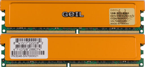
Module exterior
Module Part Number
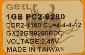
The manufacturer's web site does not publish the DDR2 Part Number expansion. The description page runs that it's a dual channel kit of PC2-9280 DDR2 memory modules with the ultra low latency of 4-4-4-12. This product comes in limited supply of 1 GB and 2 GB modules. These modules are based on 64Mx8 FBGA DDR2 chips certified for overclocking (GeIL OC Certified). Module voltage is record-breakingly high - 2.45 V.
SPD data
General SPD standard description:
DDR2 SPD standard specification:
| Parameter |
Byte |
Value |
Interpretation |
| Fundamental Memory Type |
2 |
08h |
DDR2 SDRAM |
| Number of Row Addresses on this assembly |
3 |
0Eh |
14 (RA0-RA13) |
| Number of Column Addresses on this assembly |
4 |
0Ah |
10 (CA0-CA9) |
| Number of DIMM Banks |
5 |
61h |
2 physical banks |
| Data Width of this assembly |
6 |
40h |
64 bit |
| Power supply voltage |
8 |
05h |
SSTL 1.8V |
| SDRAM Cycle time (tCK) at maximum supported CAS# latency (CL X) |
9 |
25h |
2.50 ns (400.0 MHz) |
| DIMM configuration type |
11 |
00h |
Non-ECC |
| Refresh Rate/Type |
12 |
82h |
7.8125 ms - 0.5x reduced self-refresh |
| Primary SDRAM Width (organization type) of the memory module chips |
13 |
08h |
x8 |
| Error Checking SDRAM Width (organization type) of the memory chips in the ECC module |
14 |
00h |
Not defined |
| Burst Lengths Supported (BL) |
16 |
0Ch |
BL = 4, 8 |
| Number of Banks on SDRAM Device |
17 |
04h |
4 |
| CAS Latency (CL) |
18 |
38h |
CL = 5, 4, 3 |
| Minimum clock cycle (tCK) at reduced CAS# latency (CL X-1) |
23 |
3Dh |
3.75 ns (266.7 MHz) |
| Minimum clock cycle (tCK) at reduced CAS# latency (CL X-2) |
25 |
50h |
5.00 ns (200.0 MHz) |
| Minimum Row Precharge Time (tRP) |
27 |
32h |
12.5 ns
5.0, CL = 5
3.3, CL = 4
2.5, CL = 3 |
| Minimum Row Active to Row Active delay (tRRD) |
28 |
1Eh |
7.5 ns
3.0, CL = 5
2.0, CL = 4
1.5, CL = 3 |
| Minimum RAS to CAS delay (tRCD) |
29 |
32h |
12.5 ns
5.0, CL = 5
3.3, CL = 4
2.5, CL = 3 |
| Minimum Active to Precharge Time (tRAS) |
30 |
2Dh |
45.0 ns
18.0, CL = 5
12.0, CL = 4
9.0, CL = 3 |
| Module Bank Density |
31 |
80h |
512 MB |
| Write recovery time (tWR) |
36 |
3Ch |
15.0 ns
6.0, CL = 5
4.0, CL = 4
3.0, CL = 3 |
| Internal write to read command delay (tWTR) |
37 |
1Eh |
7.5 ns
3.0, CL = 5
2.0, CL = 4
1.5, CL = 3 |
| Internal read to precharge command delay (tRTP) |
38 |
1Eh |
7.5 ns
3.0, CL = 5
2.0, CL = 4
1.5, CL = 3 |
| SDRAM Device Minimum Active to Active/Auto Refresh Time (tRC) |
41, 40 |
39h, 00h |
57.0 ns
22.8, CL = 5
15.2, CL = 4
11.4, CL = 3 |
| SDRAM Device Minimum Auto-Refresh to Active/Auto-Refresh Command Period (tRFC) |
42, 40 |
69h, 00h |
105.0 ns
42.0, CL = 5
28.0, CL = 4
21.0, CL = 3 |
| Maximum device cycle time (tCKmax) |
43 |
80h |
8.0 ns |
| SPD Revision |
62 |
12h |
Revision 1.2 |
| Checksum for Bytes 0-62 |
63 |
28h |
40 (true) |
| Manufacturer’s JEDEC ID Code |
64-71 |
7Fh, 7Fh,
7Fh, 13h |
Golden Empire |
| Module Part Number |
73-90 |
- |
CL4-4-4DDR2-1160 |
| Module Manufacturing Date |
93-94 |
06h, 27h |
Year 2006, Week 39 |
| Module Serial Number |
95-98 |
00h, 00h,
00h, 00h |
Not defined |
It seems that SPD data do not have any peculiarities. Three different CAS# latencies are supported - 5, 4, and 3. The first of the supported values (CL X) corresponds to DDR2-800 (2.5 ns cycle time) with 5-5-5-18 timings. The second value (CL X-1) is meant for DDR2-533 mode with 3.75 ns cycle time and 4-4-4-12 timings. The third value (CL X-2) - DDR2-400 mode (5.0 ns cycle time) with 3-3-3-9 timings. The manufacturer identification code and the manufacturing date are stated correctly, the part number looks like "CL4-4-4DDR2-1160", which contains the unofficial operating mode of these modules. There is no info about the serial number.
The non-standard part of the SPD (EPP profiles), represented by Bytes 99-127, is not included in our modules under review.
Testbed configuration
Testbed 1
- CPU: AMD Athlon 64 X2 5200+ (Socket AM2), nominal frequency - 2.6 GHz (200 x13)
- Chipset: NVIDIA nForce 590 SLI
- Motherboard: ASUS CROSSHAIR, BIOS 0702 dated 20.06.2007
Test results
The modules were tested on the AMD platform - AMD Athlon 64 X2 5200+ processor and ASUS CROSSHAIR motherboard (Testbed 1). We ran the tests in two modes - nominal DDR2-800 mode (2.4 GHz CPU clock, 400 MHz bus clock) and overclocked to DDR2-1160, recommended by the manufacturer (2.9 GHz CPU clock, 580 MHz bus clock).
| Parameter |
Testbed 1 |
CPU clock, MHz
(FSB clock x FID) |
2400
(200x12) |
2900
(290x10) |
Memory frequency, MHz
(DDR2 MHz) |
400
(800) |
580
(1160) |
| Default memory timings, voltage |
5-5-5-18-2T,
1.8 V |
5-5-5-18-2T,
2.45 V |
| Minimal memory timings, voltage |
3-3-3-2T,
2.45 V |
4-4-4-2T,
2.45 V |
Average memory read bandwidth, GB/sec,
1 core |
3.93
(4.10) |
4.98
(5.07) |
Average memory write bandwidth, GB/sec,
1 core |
3.30
(3.45) |
4.16
(4.28) |
Max. memory read bandwidth, GB/sec,
1 core |
7.78
(8.08) |
9.68
(9.79) |
Max. memory write bandwidth, GB/sec,
1 core |
6.73
(6.76) |
8.11
(8.11) |
Average memory read bandwidth, GB/sec,
2 cores |
6.62
(6.83) |
8.45
(8.67) |
Average memory write bandwidth, GB/sec,
2 cores |
4.06
(4.27) |
5.51
(5.70) |
Max. memory read bandwidth, GB/sec,
2 cores |
8.56
(9.10) |
11.37
(11.71) |
Max. memory write bandwidth, GB/sec,
2 cores |
6.46
(6.67) |
7.92
(8.07) |
| Minimum pseudo-random access latency, ns |
28.1
(26.2) |
21.7
(20.9) |
| Minimum random access latency*, ns |
79.8
(73.8) |
62.3
(60.0) |
*32 MB block size
The default timings scheme used by the ASUS CROSSHAIR motherboard in DDR2-800 mode matches 5-5-5-18 timings from SPD (addr CMD rate equals 2T, a typical value for the 2 GB kit). The minimum timing scheme with memory voltage increased to 2.45 V (recommended by the manufacturer) is 3-3-3 (that is it matches the minimum possible scheme for this platform; changing tRAS does not affect memory operation, as usual). This scheme increases memory bandwidth (by up to 6%) and reduces latencies (by up to 8%).
The unofficial "DDR2-1160" mode uses a 290 MHz FSB (2.9 GHz) and the default timing scheme of 5-5-5-18. In our tests we managed to reduce it to 4-4-4 (these values are specified by the manufacturer for this mode). Any attempts to reduce them even further resulted in system failures. Nevertheless, this reduction of timings has an insignificant effect on memory bandwidth (2% gain) and latencies (4% reduction). It's weaker than the effect from reducing timings from 5-5-5 to 3-3-3 in the standard DDR2-800 mode. Thus, trying to use minimum possible timings is of purely theoretical interest in both cases, at least on our AMD platform.
Bottom line
The GeIL DDR2-1160 PC2-9280 Ultra Plus Dual Channel kit consists of high-speed DDR2 memory modules compatible with our AMD AM2 platform. Memory performance and latency values are typical of modules of this speed group. Timing overclocking potential in the standard DDR2-800 mode is on the usual level - the minimum timing scheme is 3-3-3 at 2.45 V. In the fastest DDR2-1160 mode, our modules could work with 4-4-4 timings recommended by the manufacturer.
Write a comment below. No registration needed!
|
|
 |
|
|
|