 |
||
|
||
| ||
|
||
|
||
| ||
We proceed with the series of articles, dedicated to the low level analysis of the most important characteristics of DDR memory modules using our RightMark Memory Analyzer test package. Today we are going to review another high-speed offer from Corsair, probably the last DDR product — a dual-channel kit of memory (2 x 1 GB) that can operate at up to 275 MHz (DDR-550). Manufacturer InformationModule manufacturer: Corsair Memory
Module ExteriorPhoto of the memory module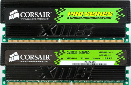
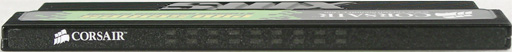 Exterior of TWINX2048-4400PRO modules is usual for the PRO series. We already examined similar DDR memory modules - TWINX2048-3500LLPRO. Distinctive features of this series are a massive aluminum heatsink (our samples are equipped with a black heatsink) and memory activity LEDs (these modules as well as TWINX2048-3500LLPRO use 18 LEDs). You can see them on the photo below (end face view). I remind you that these LEDs do not display activity of individual logical banks, but the overall load of the memory bus in a module — from minimal, indicated by the first three couples of green LEDs, to medium (three couples of yellow LEDs in the middle) and up to maximum (the last three couples of red LEDs). Module Part Number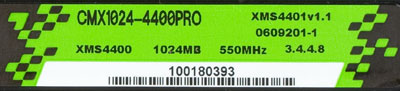 The manufacturer's web site does not publish the DDR Part Number expansion of XMS PRO series memory modules. Datasheet on these modules states that this product is a complex of two DDR-400 modules, adjusted to each other, with the total capacity of 2GB. The modules can operate at up to 275 MHz (DDR2-550 mode) using moderate timings (3-4-4-8) and 2.8V voltage. At the same time, the standard mode written in SPD chip is DDR-400 and 3-3-3-8 timings. SPD chip dataDescription of the general SPD standard:
Description of the specific SPD standard for DDR:
SPD data look rather typical for DDR-400 modules (note that faster DDR modes are not ratified by JEDEC and thus they are unofficial). Three CAS# latency values are supported — 3.0, 2.5, and 2.0. Only the first value is relevant these days — it corresponds to the 5.0ns cycle time, that is DDR-400 mode. The full timing scheme for this case is 3-3-3-9, it differs from the official scheme (3-3-3-8). The other two CAS# latencies (CL X-0.5 = 2.5 and CL X-1 = 2.0) correspond to DDR-333 and DDR-266 modes correspondingly. Timing schemes for these cases are not always written in fractional form, namely 2.5-2.5-2.5-7.5 (rounded up to 2.5-3-3-8) and 2-2-2-6 correspondingly. Manufacturer’s JEDEC ID Code and Part Number of the modules are correct. Note that the latter (CMX1024-4400PRO) does not belong to the dual-channel kit (TWINX2048-4400PRO), but to its individual components — 1 GB XMS-4400PRO memory modules. At the same time, information on the manufacturing date and serial number of the modules, as well as SPD Revision are not available. Testbed configurationsTestbed 1
Testbed 2
Testbed 3
Testbed 4
Test ResultsPerformance testsThe first series of tests was carried out with standard timings (that is the timings were set by default in BIOS) in three modes: standard DDR-400 mode (Testbed 1), maximal semi-official DDR-500 mode (that is memory operates at its maximum - 250 MHz) at maximum possible real frequency of 240 MHz obtainable when the clock frequency reaches 2.4 GHz (Testbed 2); and finally, the maximum unofficial DDR-550 mode (the CPU bus is overclocked to 230x12 ~= 2.75 GHz, memory frequency is set to its maximum - 250 MHz, which sets the real memory frequency to 2750/10 = 275 MHz, Testbed 3). We compared results of our tests in DDR-400 mode with those of high-speed dual-channel 1GB kit of Corsair XMS-3200 modules that had been tested in similar conditions (Testbed 4).
Standard memory timings (3-3-3-8) in DDR-400 mode, used by the ASUS A8N32 SLI Deluxe motherboard, turned out to be very close to SPD values (3-3-3-9). To all appearances, more conservative latencies of the command interface (2T) were chosen out of memory stability reasons. Note that the same mode was used in Corsair XMS-3200 modules, much "easier" in terms of loads on the memory controller interface. Unfortunately, this motherboard is unreasonably overcautious. Comparison of the XMS-4400PRO under review and the XMS-3200 shows that the former modules are a tad slower than the latter — it's especially noticeable in their random access latencies. That must be the effect of slower timings, used by default (3-3-3-8 versus 2-2-2-5). Nevertheless, maximal efficiency of using the memory bus in both cases is similar - approximately 96%. Still more conservative timings are set by default in semiofficial DDR-500 mode with the real memory frequency of 240 MHz, — 3-4-4-10-2T. A faster mode results in insignificant reductions of latencies and, naturally, in increased maximum real memory bandwidth - up to ~7.0 GB/s. As the theoretical memory bandwidth of the dual-channel 240MHz DDR memory is 7.68 GB/s, efficiency of using the memory bus in this case is a tad lower - approximately 91%. Timings for the extreme DDR-550 mode (275 MHz memory) are the same — 3-4-4-10-2T. There is nothing surprising about it — the motherboard still "thinks" that the memory operates at 250 MHz (as in the previous case) and sets the proper (in its opinion) timings. Due to the noticeable increase in the memory clock (from 240 MHz to 275 MHz) and the same timings, this mode demonstrates much lower latencies — they are even lower than in the XMS-3200 modules in the standard DDR-400 mode and minimal timings (2-2-2-5) both for pseudo-random and random walks. Maximum real memory bandwidth is ~8.0 GB/s. Considering the theoretical limit of 8.8 GB/s, it also amounts to 91% efficiency of memory bus usage. Stability testsMemory timings, except for tCL, were adjusted "on the fly" with the built-in RMMA feature that allows to change memory settings dynamically. Memory operating stability was evaluated with an auxiliary utility RightMark Memory Stability Test, included into RMMA.
Minimal timings for the new XMS-4400PRO modules are identical to those for the XMS-3500LLPRO, including additional parameters (tRC and tRFC) — 2-3-2-5(-7-10). Of course, the modules worked well with lower command interface latencies (1T), so our motherboard BIOS is overcautious here. Compared to the nominal values, such extreme settings help increase the real memory bandwidth (they raise the efficiency of using the bus to 98%) and reduce latencies, which nearly reached the XMS-3200 values for pseudo-random memory access. Increased memory bandwidth and reduced latencies are also demonstrated in DDR-500 mode (240 MHz memory clock) with the following minimum stable timings - 2.5-3-3-5-7-12-1T. Note that the system remained efficient even with 2.5-3-2-5 timings, but in this case our memory stability test detected frequent errors. The ultimate DDR-550 mode is no less interesting, it allows to reduce timings to 3-4-3-5-7-13-2T. By the way, tRAS and tRC values seem to be ignored by these modules like most other DDR/DDR2 memory modules. Indeed, tRAS/tRC = 5/7 values look quite unreal. At the same time, you can see well that the memory system is sensitive to tRFC changes. In this case it equals 13 (versus 10 in DDR-400 mode, both for XMS-4400PRO and XMS-3200 modules). What concerns operating stability, the system seemed to work well even with 1T command interface delays and "harder" timings (3-3-3-5-7-13-2T). But in both cases our memory stability test detected errors rather quickly. Thus, the minimal timings scheme for this case is 3-4-3-2T. Not bad — not all DDR2-533 memory modules (with similar or worse speed characteristics) can work with such timings. Bottom lineCorsair XMS-4400PRO modules are a typical offer among high-speed capacious DDR modules that can work well in the standard DDR-400 mode with fast 2-3-2-1T timings. In this mode, our modules demonstrate 98% efficiency of memory bus usage. The modules demonstrate a good overclocking potential both at maximum 240 MHz in standard conditions (minimal timings - 2.5-3-3-1T) and in maximum frequency mode - 275 MHz (minimal timings — 3-4-3-2T). The modules are still notable for high efficiency of memory bus utilization, about 91%.
Corsair TWINX2048-4400PRO Modules are kindly provided by the representative office of Corsair Memory in Russia Dmitri Besedin (dmitri_b@ixbt.com) August 18, 2006. Write a comment below. No registration needed!
|
Platform · Video · Multimedia · Mobile · Other || About us & Privacy policy · Twitter · Facebook Copyright © Byrds Research & Publishing, Ltd., 1997–2011. All rights reserved. |


