Chaintech Apogee GT DDR2-800+ (PC2-6400) Low-Latency Memory Modules
|
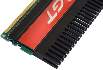
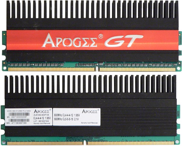
Today we are going to take a look at memory modules by Chaintech. This company is well known to our readers as a manufacturer of graphics cards, and, in the past, motherboards. What we see is small, by modern standards, capacity of a mere 1 GB. However, it's still adequate for the users of middle-end systems not rushing to switch Vista and preferring Windows XP or Linux instead. Besides, the modules have reduced timings and a cooling system similar to Corsair's patented DHX. Having no additional contact with the module's circuit board, the cooling system only contacts the chips' surfaces.
Manufacturer Information
Module manufacturer: Walton Chaintech Corporation
Chip manufacturer: unknown
Module manufacturer's website: Walton Chaintech
Module's Exterior
Module's Part Number
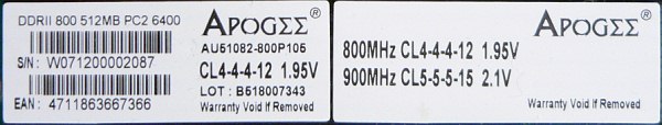
Part number guide for the DDR2 memory modules could not be found on the manufacturer's website. The description on the website is more than brief. With additional help of the markings on the modules themselves we can determine that the product is a set of two low-latency modules (CL4) of 512 KB each. They are based on 16 BGA packed microchips in a 64M x 8 configuration. The manufacturer guarantees stable operation of the modules in DDR2-800 mode with timings of 4-4-4-12 and a supply voltage of 1.95 V, as well as DDR2-900 mode with timings of 5-5-5-15 and a supply voltage of 2.1 V. The SPD microchip uses DDR2-800 with timings of 5-5-5-15 and a supply voltage of 1.8 V as the default mode.
SPD Data
General SPD standard specifications:
DDR2 SPD standard specifications:
| Parameter |
Byte |
Value |
Interpretation |
| Fundamental memory type |
2 |
08h |
DDR2 SDRAM |
| Total number of address lines per module's row |
3 |
0Eh |
14 (RA0-RA13) |
| Total number of address lines per module's column |
4 |
0Ah |
10 (CA0-CA9) |
| Total number of physical banks in memory module |
5 |
60h |
1 physical bank |
| External data bus of memory module |
6 |
40h |
64 bit |
| Power supply voltage |
8 |
05h |
SSTL 1.8V |
| Minimum length of clock signal period (tCK) with maximum CAS# latency (CL X) |
9 |
25h |
2.50 ns (400 MHz) |
| Module configuration type |
11 |
00h |
Non-ECC |
| Type and method of data recovery |
12 |
02h |
Clearly, «82h» was meant here, which corresponds to a value of 7.8125 ms - 0.5x reduced self-recovery |
| External interface data bus width (organization type) of memory chips being used |
13 |
08h |
x8 |
| External interface data bus width (organization type) of ECC-module memory chips being used |
14 |
00h |
Indeterminate |
| Burst length (BL) |
16 |
0Ch |
BL = 4, 8 |
| Number of logical banks for each chip in module |
17 |
04h |
4 |
| Supported CAS# latency durations (CL) |
18 |
38h |
CL = 5, 4, 3 |
| Minimum length of clock signal period (tCK) with reduced CAS# latency (CL X-1) |
23 |
3Dh |
3.75 ns (266.7 MHz) |
| Minimum length of clock signal period (tCK) with reduced CAS# latency (CL X-2) |
25 |
50h |
5.00 ns (200.0 MHz) |
| Minimum row precharge time (tRP) |
27 |
32h |
12.5 ns
5, CL = 5
3.33, CL = 4
2.5, CL = 3 |
| Minimum row to row delay (tRRD) |
28 |
1Eh |
7.5 ns
3, CL = 5
2, CL = 4
1.5, CL = 3 |
| Minimum delay between RAS# and CAS# (tRCD) |
29 |
32h |
12.5 ns
5, CL = 5
3.33, CL = 4
2.5, CL = 3 |
| Minimum pulse length of RAS# signal (tRAS) |
30 |
25h |
37.0 ns
15, CL = 5
10, CL = 4
7.4, CL = 3 |
| Capacity of one physical bank of memory module |
31 |
80h |
512 MB |
| Write recovery time (tWR) |
36 |
3Ch |
15.0 ns
6, CL = 5
4, CL = 4
3, CL = 3 |
| WRITE to READ time (tWTR) |
37 |
1Eh |
7.5 ns
3, CL = 5
2, CL = 4
1.5, CL = 3 |
| READ to PRECHARGE time (tRTP) |
38 |
1Eh |
7.5 ns
3, CL = 5
2, CL = 4
1.5, CL = 3 |
| Minimum row cycle time (tRC) |
41, 40 |
39h, 30h |
57.5 ns
23, CL = 5
15.3, CL = 4
11.5, CL = 3 |
| Period between self-recovery commands (tRFC) |
42, 40 |
69h, 30h |
105.0 ns
42, CL = 5
28, CL = 4
21, CL = 3 |
| Maximum length of clock signal period (tCKmax) |
43 |
80h |
8.0 ns |
| SPD revision number |
62 |
12h |
Revision 1.2 |
| Checksum for bytes 0-62 |
63 |
D3h |
211 (correct) |
| Manufacturer identification code according to JEDEC |
64-71 |
00h, 00h |
Indeterminate |
| Module's part number |
73-90 |
- |
NU5108E32-800P100 |
| Module's manufacture date |
93-94 |
07h, 10h |
year 2007, week 16 |
| Module's serial number |
95-98 |
F0h, 31h,
0Bh, 14h |
140B31F0h |
The SPD supports all three of the possible CAS# signal latency values - 5, 4 and 3. The first one (CL X = 5) corresponds to operating in DDR2-800 mode (2.5 ns cycle time, 400 MHz frequency) with a timing scheme of 5-5-5-15 (exactly). The second CAS# signal latency value (CL X-1 = 4) corresponds to DDR2-533 mode (3.75 ns cycle time, 266.7 MHz frequency) with a non-standard timing scheme of 4-3.27-3.27-10. Finally, the last CAS# signal latency value (CL X-2 = 3) corresponds to DDR2-400 mode, also with a non-integer timing scheme of 3-2.5-2.5-7.4.
It is quite strange that a rather popular DDR2-667 mode is not supported. Even more so, because we had no problem manually setting this mode with the typical timing scheme of 4-4-4-12 and standard voltage.
SPD revision number and checksum are specified correctly. Manufacturer identification code is missing, while the module's part number is not quite what is marked on the modules themselves.
SPD standard EPP extensions are not supported by the modules under consideration.
Testbed Configuration
- CPU: AMD Athlon 64 X2 4000+ (Socket AM2), 2.0 GHz (200 x10)
- Chipset: NVIDIA nForce 590 SLI
- Motherboard: ASUS M2N32 WS Professional, BIOS version 1601 (10/08/2007)
Test Results
We pursued two goals while testing the modules. The first goal was to achieve maximum frequency while using the minimal recommended timing scheme (4-4-4-12). To that end we tested the modules first with the recommended voltage of 1.95 V. Next, we increased FSB frequency and voltage. The voltage upper bound was set at 2.3 V, which is relatively safe for the modern DDR2 chips (provided appropriate heat removal). In the second part of the test we set the recommended elevated frequency that corresponded to DDR2-900 with the timing scheme of 5-5-5-15 and voltage of 2.1 V. Again, we increased the frequency and voltage up to 2.3 V in order to determine the frequency upper bound for the given modules.
| |
Chaintech Apogee GT DDR2-800+ |
CPU clock rate, MHz
(FSB frequency x FID) |
2000
(200x10) |
2000
(200x10) |
2120
(212x10) |
2250
(225x10) |
2330
(233x10) |
Memory frequency, MHz
(DDR2 MHz) |
400
(800) |
400
(800) |
424
(848) |
450
(900) |
466
(932) |
| Memory timings by default, voltage |
5-5-5-15-1T,
1.8 V |
4-4-4-12-1T,
1.95 V |
4-4-4-12-1T,
2.3 V |
5-5-5-15-2T,
2.1 V |
5-5-5-15-2T,
2.3 V |
| Minimum memory timings, voltage |
(not tested) |
same,
up to 2.3 V |
(not tested) |
same,
up to 2.3 V |
(not tested) |
Average read bandwidth (MB/s),
1 core |
3494 |
3608 |
3802 |
3857 |
3997 |
Average write bandwidth (MB/s),
1 core |
1982 |
2053 |
2165 |
2211 |
2295 |
Max. read bandwidth (MB/s),
1 core |
6605 |
6617 |
6982 |
7198 |
7453 |
Max. write bandwidth (MB/s),
1 core |
5706 |
5717 |
6033 |
6380 |
6607 |
Average read bandwidth (MB/s),
2 cores |
6315 |
6506 |
6924 |
6778 |
7008 |
Average write bandwidth (MB/s),
2 cores |
3106 |
3197 |
3412 |
3222 |
3347 |
Max. read bandwidth (w/PF, MB/s),
2 cores |
9260 |
9811 |
10367 |
9620 |
9913 |
Max. write bandwidth (NT, MB/s),
2 cores |
5184 |
5604 |
5924 |
5762 |
5970 |
| Minimum pseudorandom access latency, ns |
30.4 |
29.0 |
27.5 |
28.4 |
27.4 |
| Minimum random access latency*, ns |
87.8 |
85.2 |
80.7 |
82.1 |
79.3 |
| DOOM III (Low@640x480), fps |
114.8 |
116.2 |
123.1 |
127.2 |
131.7 |
| FarCry (Low@640x480), fps |
166.7 |
170.0 |
178.8 |
182.1 |
188.3 |
*for a 32 MB block size
We were pleased with the stable operation of the memory modules in reduced timing modes. Not only have they demonstrated acceleration to 424 MHz, but have proven to be capable of operating at such frequency with command interface latency parameter set to 1T. At the same time, with the frequency of 450 MHz, despite setting the timings to the standard scheme of 5-5-5-15, we have only been able to achieve stable operation by setting the aforementioned parameter to 2T. The maximum frequency produced by overclocking with higher voltage has not impressed us: a mere 16 MHz above nominal.
However, if we look at the objective RMMA results, it turns out that of the two modes recommended by the manufacturer the second one (DDR2-900) surpasses the first one by all parameters. It is true even if we take latency into account, and despite the "mediocre" timings used with the second mode. In addition, we come to the same conclusion while comparing the two modes after overclocking.
It is quite natural that the game test results support the finding presented above. In our case such results are additionally affected by the elevated CPU clock rate in modes where memory frequency is above 400 MHz.
Conclusion
Despite the fact that the active users are getting ready to make the transition to memory packages of 2 and even 4 GB in capacity, a certain demand for relatively small memory modules remains. The reason is simply that 1 GB of RAM is quite enough for work and, to some degree, games for users of a Windows XP or a Linux computer. Apart from the difference in price, the smaller modules usually have better latency characteristics. They allow setting extreme timing schemes for the standard frequency mode (DDR2-800). The users, who do not want to increase CPU clock rate above nominal, but would like to use the memory's full potential, are bound to appreciate that. At the same time a better strategy for those, who are not prejudiced against overclocking, would be raising the memory frequency to the maximum possible value, even at the cost of having to use a moderate timing scheme.
Write a comment below. No registration needed!
|
|
 |
|
|
|


