Memory Module Analysis. Part 17: Apacer DDR2-667 Modules
|
We proceed with the low-level analysis of the most important characteristics of DDR2 memory modules using our RightMark Memory Analyzer. In this review we shall examine a 1GB pair of DDR2-667 modules from Apacer — quite a common offer in this category for these days.
Manufacturer Information
Module manufacturer: Apacer Technology Inc.
Manufacturer of module chips: Elpida Memory, Inc.
Web site of the module manufacturer:
http://www.apacer.com/en/products/Desktop_Memory_DDR2.htm
Web site of the chip manufacturer:
http://www.elpida.com/en/products/ddr2.html
Module Exterior
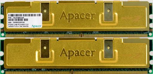
Photo of the memory module
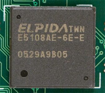
Photo of the memory chip
Stylish golden heatsink of a standard design covers a usual memory "bar" with eight DDR2 memory chips manufactured by Elpida.
It's important to note that the heatsink itself is mostly just a decoration. As you can see on the photo above, the sticky heat-conducting layer does not touch most memory chips on the edges of the module — the only exception is two, maximum four, chips in the center. Pay attention that these are production-line modules, not engineering samples. The problem has to do with quite a wide heatsink, evidently intended for cooling chips on two-bank memory modules. Solution to this problem is trivial — use a thicker layer (not necessarily possessing high heat-conductivity) on the back of a module. Nevertheless, the manufacturer hasn't taken the trouble to do it yet for some reasons. Let's hope that the situation will change in future.
Module and Chip Part Number
Module Part Number Expansion
There is no DDR2 part number expansion as well as any technical documentation on these products on the official web site. Nevertheless, expansion of a module designation is evident — this product is a 512 MB unbuffered PC2-5300 (that is DDR2-667) memory module, operating with CAS# latency tCL = 5.
Chip Part Number Expansion
Data sheet on 512 Mbit DDR2 Elpida memory chips: http://www.elpida.com/pdfs/E0562E61.pdf
| Field |
Value |
Expansion |
| 0 |
E |
Manufacturer: E = Elpida Memory |
| 1 |
|
Type (n/a, D = monolithic device) |
| 2 |
|
Product code (n/a, E = DDR2) |
| 3 |
51 |
Density/Bank: 51 = 512 Mbit/4 banks
|
| 4 |
08 |
Bit organization: 08 = x8 |
| 5 |
A |
Power supply, Interface: A = SSTL
1.8V |
| 6 |
E |
Die revision |
| 7 |
|
Package code (n/a, SE = FBGA) |
| 8 |
6E |
Speed: 6E = DDR2-667 (5-5-5) |
| 9 |
E |
Environment code: E = lead free |
Chip designation of this module does not comply with the official specification, provided in the technical documentation on this type of chips. Namely, there are no fields with the device type (monolithic, DDR2) and package (FBGA). We have already seen it in other DDR2 memory modules with Elpida chips, for example, in budget DDR2 Kingston ValueRAM modules.
SPD chip data
Description of the general SPD standard:
Description of the specific SPD standard for DDR2:
| Parameter |
Byte |
Value |
Expansion |
| Fundamental Memory Type |
2 |
08h |
DDR2 SDRAM |
| Number of Row Addresses on this assembly |
3 |
0Eh |
14 (RA0-RA13) |
| Number of Column Addresses on this assembly |
4 |
0Ah |
10 (CA0-CA9) |
| Number of DIMM Banks |
5 |
60h |
1 physical bank |
| Data Width of this assembly |
6 |
40h |
64 bit |
| Voltage Interface Level of this assembly |
8 |
05h |
SSTL 1.8V |
| SDRAM Cycle time (tCK) at maximum supported
CAS# latency (CL X) |
9 |
30h |
3.00 ns (333.3 MHz) |
| DIMM configuration type |
11 |
00h |
Non-ECC |
| Refresh Rate/Type |
12 |
82h |
7.8125 ms — 0.5x reduced self-refresh |
| Primary SDRAM Width (organization type) of the
memory module chips |
13 |
08h |
x8 |
| Error Checking SDRAM Width (organization type)
of the memory chips in the ECC module |
14 |
00h |
Not defined |
| Burst Lengths Supported (BL) |
16 |
0Ch |
BL = 4, 8 |
| Number of Banks on SDRAM Device |
17 |
04h |
4 |
| CAS Latency (CL) |
18 |
38h |
CL = 5, 4, 3 |
| Minimum clock cycle (tCK) at reduced
CAS# latency (CL X-1) |
23 |
3Dh |
3.75 ns (266.7 MHz) |
| Minimum clock cycle (tCK) at reduced
CAS# latency (CL X-2) |
25 |
50h |
5.00 ns (200.0 MHz) |
| Minimum Row Precharge Time (tRP) |
27 |
3Ch |
15.0 ns
5, CL = 5
4, CL = 4
3, CL = 3 |
| Minimum Row Active to Row Active delay (tRRD) |
28 |
1Eh |
7.5 ns
2.5, CL = 5
2.0, CL = 4
1.5, CL = 3 |
| Minimum RAS to CAS delay (tRCD) |
29 |
3Ch |
15.0 ns
5, CL = 5
4, CL = 4
3, CL = 3 |
| Minimum Active to Precharge Time (tRAS) |
30 |
2Dh |
45.0 ns
15, CL = 5
12, CL = 4
9, CL = 3 |
| Module Bank Density |
31 |
80h |
512 MB |
| Write recovery time (tWR) |
36 |
3Ch |
15.0 ns
5, CL = 5
4, CL = 4
3, CL = 3 |
| Internal write to read command delay (tWTR) |
37 |
1Eh |
7.5 ns
2.5, CL = 5
2.0, CL = 4
1.5, CL = 3 |
| Internal read to precharge command delay (tRTP) |
38 |
1Eh |
7.5 ns
2.5, CL = 5
2.0, CL = 4
1.5, CL = 3 |
| SDRAM Device Minimum Active to Active/Auto Refresh
Time (tRC) |
41, 40 |
3Ch, 00h |
60.0 ns
20, CL = 5
16, CL = 4
12, CL = 3 |
| SDRAM Device Minimum Auto-Refresh to Active/Auto-Refresh
Command Period (tRFC) |
42, 40 |
69h, 00h |
105.0 ns
35, CL = 5
28, CL = 4
21, CL = 3 |
| Maximum device cycle time (tCKmax) |
43 |
80h |
8.0 ns |
| SPD Revision |
62 |
12h |
Revision 1.2 |
| Checksum for Bytes 0-62 |
63 |
DDh |
221 (true) |
| Manufacturer’s JEDEC ID Code |
64-71 |
7Fh, 7Ah |
Apacer Technology |
| Module Part Number |
73-90 |
FFh...FFh |
Wrong |
| Module Manufacturing Date |
93-94 |
FFh, FFh |
Wrong |
| Module Serial Number |
95-98 |
FFh, FFh,
FFh, FFh |
Wrong |
SPD contents, that have to do with memory timings, look standard for a DDR2-667 module. All three CAS# latencies are supported — 5, 4, and 3. The first value corresponds to the cycle time of 3.0 ns (333.3 MHz, DDR2-667), timings for this case correspond to the first official DDR2-667 standard — 5-5-5-15 (later versions of this standard allow a faster scheme - 4-4-4-12). Reduced CAS# latency (CL X-1 = 4) corresponds to the 3.75 ns cycle time (DDR2-533) and 4-4-4-12 timings, currently slightly outdated for this mode as well. And finally the last CAS# latency (CL X-2 = 3) corresponds to the cycle time of 5.0 ns (that is DDR2-400) and 3-3-3-9 timings. We can also note a slightly increased minimum refresh to active/refresh command period (tRFC = 105 ns), which conforms well with the overall conservative nature of timings in these modules. SPD revision number and Manufacturer’s JEDEC ID Code are correct. At the same time, there are no adequate data on Part Number, manufacturing date, and serial number of the module — all these fields contain FFh codes.
Testbed configurations
Testbed 1
- CPU: Intel Pentium 4 Extreme Edition 3.73 GHz (Prescott N0, 2 MB L2) operating at 2.8 GHz (200.0 MHz x14)
- Chipset: Intel 975X
- Motherboard: ASUS P5WD2-E Premium, BIOS 0206 dated 12/21/2005
- Memory: 2x512 MB Apacer DDR2-667
Testbed 2
- CPU: Intel Pentium 4 Extreme Edition 3.73 GHz (Prescott N0, 2 MB L2) operating at 3.73 GHz (266.7 MHz x14)
- Chipset: Intel 975X
- Motherboard: ASUS P5WD2-E Premium, BIOS 0206 dated 12/21/2005
- Memory: 2x512 MB Apacer DDR2-667
Test Results
Performance tests
In the first series of tests we used the timing scheme, set in BIOS Setup by default (Memory Timings: "by SPD"). The ASUS P5WD2-E motherboard, we used for these tests, set it by SPD.
| Parameter |
Testbed 1 |
Testbed 2* |
| Timings |
5-5-5-15 |
5-5-5-15 |
| Average memory read bandwidth,
MB/sec |
5383 |
6400 |
| Average memory write bandwidth,
MB/sec |
2101 |
2296 |
| Max. memory read bandwidth,
MB/sec |
6633 |
8342 |
| Max. memory write bandwidth,
MB/sec |
4282 |
5677 |
| Minimum Pseudo-Random
Access Latency, ns |
56.6 |
50.1 |
| Maximum Pseudo-Random
Access Latency, ns |
66.1 |
57.2 |
| Minimum Random Access
Latency**, ns |
116.2 |
102.9 |
| Maximum Random Access
Latency**, ns |
140.4 |
121.0 |
Minimum Pseudo-Random
Access Latency, ns
(without hardware prefetch) |
87.2 |
77.8 |
Maximum Pseudo-Random
Access Latency, ns
(without hardware prefetch) |
113.0 |
96.4 |
Minimum Random Access
Latency**, ns
(without hardware prefetch) |
117.0 |
104.0 |
Maximum Random Access
Latency**, ns
(without hardware prefetch) |
143.0 |
123.1 |
*266 MHz FSB
**16MB block size
Results published above show that the modules under review are characterized by mediocre performance characteristics (maximum real memory bandwidth in real tests on processors with 2 MB L2 Cache usually amounts to about 6.8 GB/s at 200 MHz FSB and about 9 GB/s at 266 MHz). The same applies to memory access latencies - they are lower with 266 MHz FSB, but still higher than typical values for high-performance DDR2-667 modules (about 70 ns for pseudo-random walks with disabled hardware prefetch — a true memory latency characteristic).
Stability tests
Timing values, except for tCL, were adjusted "on the fly" due to the built-in RMMA feature that allows to change dynamically memory settings supported by the chipset. Memory operating stability was evaluated with an auxiliary utility RightMark Memory Stability Test, included into RMMA.
| Parameter* |
Testbed 1 |
Testbed 2* |
| Timings |
4-4-4 |
4-4-4 |
| Average memory read bandwidth,
MB/sec |
5490 |
6608 |
| Average memory write bandwidth,
MB/sec |
2344 |
2681 |
| Max. memory read bandwidth,
MB/sec |
6675 |
8464 |
| Max. memory write bandwidth,
MB/sec |
4282 |
5684 |
| Minimum Pseudo-Random
Access Latency, ns |
54.5 |
47.5 |
| Maximum Pseudo-Random
Access Latency, ns |
64.0 |
55.2 |
| Minimum Random Access
Latency**, ns |
110.1 |
96.5 |
| Maximum Random Access
Latency**, ns |
134.4 |
115.6 |
Minimum Pseudo-Random
Access Latency, ns
(without hardware prefetch) |
83.7 |
73.3 |
Maximum Pseudo-Random
Access Latency, ns
(without hardware prefetch) |
109.8 |
93.1 |
Minimum Random Access
Latency**, ns
(without hardware prefetch) |
110.9 |
97.4 |
Maximum Random Access
Latency**, ns
(without hardware prefetch) |
137.5 |
116.7 |
*266 MHz FSB
**16MB block size
As you can see on the table published above, in this series of tests we managed to obtain minimum timings (4-4-4) retaining operating stability — typical values for high-performance DDR2-667 modules (the last timing, tRAS, is ignored, as usual — it can be reduced even to 4 without apparent changes). Such timings have little effect on memory bandwidth (quite expectably), but result in a reduction of memory access latencies (approximately by 3-4 ns for pseudo-random walks and by 6-7 ns for random walks).
Bottom line
Considering capacity and performance characteristics, Apacer DDR2-667 memory modules are a Middle-End solution in this category. Minimum timings supported by these modules in DDR2-667 mode (4-4-4) are rather frugal, as they are standard for modern high-performance DDR2-667 memory modules. Moreover, these production-line modules have a flaw in their design - insufficient contact between the heatsink and most memory chips on the module edges.
Write a comment below. No registration needed!
|
|
 |
|
|
|