Memory Module Analysis. Part 16: A-DATA DDR2-800 Modules
|
We proceed with the low-level analysis of the most important characteristics of high-performance DDR2 memory modules using our RightMark Memory Analyzer. Today we are going to review memory modules from a Taiwanese manufacturer A-DATA - Vitesta series, intended for 800 MHz (in DDR2 mode).
Manufacturer Information
Module manufacturer: A-DATA Technology Co., Ltd.
Manufacturer of module chips: Elpida Memory, Inc.
Web site of the module manufacturer: http://www.adata.com.tw/en/products-d-un-ddr2-800.htm
Web site of the chip manufacturer: http://www.elpida.com/en/products/ddr2.html
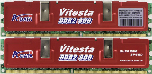
Module Exterior
Photo of the memory module
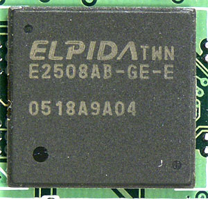
Photo of the memory chip
Interestingly, having removed a heatsink (quite an easy and painless procedure), the modules still looked decent. In particular, there are stickers with the part number and serial number on the heatsinks and on the modules themselves. Stickers on the modules also show the company's logo, but regular users will hardly make it out :).
Module and Chip Part Number
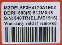
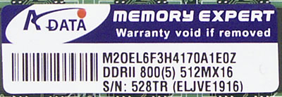
Module Part Number
It's nice that the module numbers on stickers and under them match (however, serial numbers are different). Nevertheless, there is no Part Number expansion for Vitesta DDR2 modules on the manufacturer's web site. The web page describing the modules contain only basic technical characteristics: each module is either 256 MB or (in our case) 512 MB, the modules are based on 32Mx8 chips, operating at CAS# = 5 and standard voltage = 1.85±0.1V.
Chip Part Number
Data sheet on 256-Mbit DDR2 Elpida memory chips: http://www.elpida.com/pdfs/E0657E20.pdf
| Field |
Value |
Expansion |
| 0 |
|
Manufacturer (n/a; "E" = Elpida Memory) |
| 1 |
|
Type (n/a; "D" = monolithic device) |
| 2 |
E |
Product family: "E" = DDR2 |
| 3 |
51 |
Density/Bank: "25" = 256M/4 banks |
| 4 |
08 |
Organization: "08" = x8 |
| 5 |
A |
Power supply, Interface: "A" = SSTL 1.8V |
| 6 |
B |
Die revision |
| 7 |
|
Packaging code (n/a; "SE" = FBGA) |
| 8 |
5C |
Speed: "GE" = DDR2-800 (5-5-5) |
| 9 |
E |
Environment code: "E" = Lead free |
Designation of chips in this module does not comply with the official specifications published in the data sheet on memory chips. Namely, the designation starts with a single letter "E" instead of an expected letter combination "EDE". Besides, there is no packaging type code ("SE" = FBGA packaging). However, we already came across such an approach to marking Elpida chips (for example, on Kingston DDR2 chips), so it's a rule rather than an exception.
SPD chip data
Description of the general SPD standard:
Description of the specific SPD standard for DDR2:
| Parameter |
Byte |
Value |
Expansion |
| Fundamental Memory Type |
2 |
08h |
DDR2 SDRAM |
| Number of Row Addresses on this assembly |
3 |
0Dh |
13 (RA0-RA12) |
| Number of Column Addresses on this assembly |
4 |
0Ah |
10 (CA0-CA9) |
| Number of DIMM Banks |
5 |
61h |
2 physical banks |
| Data Width of this assembly |
6 |
40h |
64 bit |
| Voltage Interface Level of this assembly |
8 |
05h |
SSTL 1.8V |
| SDRAM Cycle time (tCK) at maximum supported CAS# latency (CL X) |
9 |
25h |
2.50 ns (400.0 MHz) |
| DIMM configuration type |
11 |
00h |
Non-Parity, Non-ECC |
| Refresh Rate/Type |
12 |
82h |
7.8125 ms — 0.5x reduced self-refresh |
| Primary SDRAM Width (organization type) of the memory module chips |
13 |
08h |
x8 |
| Error Checking SDRAM Width (organization type) of the memory chips in the ECC module |
14 |
00h |
Not defined |
| Burst Lengths Supported (BL) |
16 |
0Ch |
BL = 4, 8 |
| Number of Banks on SDRAM Device |
17 |
04h |
4 |
| CAS Latency (CL) |
18 |
38h |
CL = 5, 4, 3 |
| Minimum clock cycle (tCK) at reduced CAS# latency (CL X-1) |
23 |
30h |
3.00 ns (333.3 MHz) |
| Minimum clock cycle (tCK) at reduced CAS# latency (CL X-2) |
25 |
3Dh |
3.75 ns (266.7 MHz) |
| Minimum Row Precharge Time (tRP) |
27 |
32h |
12.5 ns
5, CL = 5
~4.2, CL = 4
~3.3, CL = 3 |
| Minimum Row Active to Row Active delay (tRRD) |
28 |
1Eh |
7.5 ns
3, CL = 5
2.5, CL = 4
2, CL = 3 |
| Minimum RAS to CAS delay (tRCD) |
29 |
32h |
12.5 ns
5, CL = 5
~4.2, CL = 4
~3.3, CL = 3 |
| Minimum Active to Precharge Time (tRAS) |
30 |
2Dh |
45.0 ns
18, CL = 5
15, CL = 4
12, CL = 3 |
| Module Bank Density |
31 |
40h |
256 MB |
| Write recovery time (tWR) |
36 |
3Ch |
15.0 ns
6, CL = 5
5, CL = 4
4, CL = 3 |
| Internal write to read command delay (tWTR) |
37 |
1Eh |
7.5 ns
3, CL = 5
2.5, CL = 4
2, CL = 3 |
| Internal read to precharge command delay (tRTP) |
38 |
1Eh |
7.5 ns
3, CL = 5
2.5, CL = 4
2, CL = 3 |
| SDRAM Device Minimum Active to Active/Auto Refresh Time (tRC) |
41, 40 |
39h, 30h |
57.5 ns
23, CL = 5
~19.2, CL = 4
~15.3, CL = 3 |
| SDRAM Device Minimum Auto-Refresh to Active/Auto-Refresh Command Period (tRFC) |
42, 40 |
4Bh, 30h |
75.0 ns
30, CL = 5
25, CL = 4
20, CL = 3 |
| Maximum device cycle time (tCKmax) |
43 |
80h |
8.0 ns |
| SPD Revision |
62 |
12h |
Revision 1.2 |
| Checksum for Bytes 0-62 |
63 |
B9h |
185 (true) |
| Manufacturer’s JEDEC ID Code |
64-71 |
7Fh, 7Fh,
7Fh, 7Fh,
CBh |
A-DATA Technology |
| Module Part Number |
73-90 |
— |
Not defined |
| Module Manufacturing Date |
93-94 |
00h, 00h |
Not defined |
| Module Serial Number |
95-98 |
00h, 00h,
00h, 00h |
Not defined |
SPD contents look almost standard. The modules support all the three possible CAS# latencies — 5, 4, and 3. The maximum value corresponds to 2.50 ns cycle time (400 MHz, that is the nominal DDR2-800 mode) and the usual 5-5-5-18 timings. Reduced CAS# latency (CL X-1 = 4) is prescribed to DDR2-667 mode (3.00 ns cycle time, 333.3 MHz). Unfortunately, it's impossible to use integer timings in this case — rounding them to the nearest tenth gives 4-4.2-4.2-15, which will most likely be interpreted by BIOS as 4-5-5-15 (rounding up for stability reasons). The last value (reduced twice) tCL (CL X-2 = 3) corresponds to DDR2-533 mode (3.75 ns cycle time, 266.7 MHz). Timings for this case are also non-integer — 4-3.3-3.3-12 (that is in fact 4-4-4-12). The manufacturer's code written in SPD pleasantly corresponds to reality. Nevertheless, information on the manufacturing date, part number, and serial number is missing — it does not produce a very good impression. Testbed Configurations and Software
Testbed 1
- CPU: Intel Pentium 4 560, 3.6 GHz (Prescott core rev. E0, 1 MB L2)
- Chipset: Intel 955X, 200 MHz FSB
- Motherboard: Gigabyte 8I955X Pro, BIOS F5 dated 07/05/2005
- Memory: 2x512 MB A-DATA DDR2-800, single/dual channel
- Video: Leadtek PX350 TDH, NVIDIA PCX5900
- HDD: WD Raptor WD360, SATA, 10000 rpm, 36Gb
- Drivers: NVIDIA Forceware 77.72, Intel Chipset Utility 7.2.1.1003, DirectX 9.0c
Test Results
Performance tests
For a number of reasons, we use only one motherboard for testing A-DATA DDR2-800 modules — Gigabyte 8I955X Pro. Note that this model is one of rare motherboards, which support such fast memory as DDR2-800. Like in our previous review, we carry out our tests both in the usual dual-channel mode as well as in the single-channel mode, in order to show "pure" DDR2-800 potential (bandwidth in particular).
| Parameter |
Testbed 1 |
| Dual channel mode |
Single channel mode |
| Timings |
5-5-5-15
|
5-5-5-15
|
| Average memory read bandwidth,
MB/sec |
5799
|
5770
|
| Average memory write bandwidth,
MB/sec |
2456
|
2393
|
| Max. memory read bandwidth,
MB/sec |
6457
|
6333
|
| Max. memory write bandwidth,
MB/sec |
4279
|
4279
|
| Minimum Pseudo-Random
Access Latency, ns |
44.0
|
44.0
|
| Maximum Pseudo-Random
Access Latency, ns |
51.7
|
51.7
|
| Minimum Random Access
Latency*, ns |
93.7
|
93.9
|
| Maximum Random Access
Latency*, ns |
113.2
|
113.4
|
Minimum Pseudo-Random
Access Latency, ns
(without hardware prefetch) |
68.4
|
68.4
|
Maximum Pseudo-Random
Access Latency, ns
(without hardware prefetch) |
87.9
|
87.9
|
Minimum Random Access
Latency*, ns
(without hardware prefetch) |
94.1
|
94.3
|
Maximum Random Access
Latency*, ns
(without hardware prefetch) |
114.2
|
114.3
|
*16 MB block size
5-5-5-15 timings, set by default on this motherboard (Memory Timings: "by SPD"), is a tad different from the scheme, specified in SPD (5-5-5-18). But we can safely ignore this difference - as we have found out in the next series of tests, the modules under review are absolutely insensitive to tRAS, specified in configuration registers of the chipset, like the majority of other DDR2 modules.
Performance parameters (memory bandwidth) of the modules in dual-channel and
single-channel modes are slightly different — of course, in
favour of the dual-channel mode. The largest difference (just 2%)
is demonstrated in the test for maximum real memory read bandwidth
(6457 versus 6333 MB/s). The difference is small, but there was hardly
any difference in the previous review of Corsair
XMS2-8000UL modules. There is just a chance, of course, that is
has to do with using different processors (Pentium 4 560 and 670)
— it's quite likely that the large L2 Cache in Pentium 4 670
processor can hide the memory bandwidth differences to a larger extent.
Nevertheless, the "pure" potential of the DDR2-800 under review
(that is due to the real bandwidth of a single channel) is also quite
good.
Besides, we can enjoy quite low (noticeably lower compared to Corsair
XMS2-8000UL) memory access latencies, even with the standard timings.
Nevertheless, it's not a direct advantage of these modules over the
others — in these tests we actually used different motherboard
models (and also most importantly — different BIOS versions)
and different processors (the effect of this factor is much less probable,
but nevertheless it shouldn't be ignored). So the final answer to
the question whether the modules under review really feature lower
latencies requires additional analysis.
Stability tests
Timing values, except for tCL, were adjusted "on the fly" due to the built-in RMMA feature that allows to change dynamically memory settings supported by the chipset. Memory operating stability was evaluated with an auxiliary utility RightMark Memory Stability Test, included into RMMA.
We set a tad higher memory voltage in order to get minimal timings
— 2.2V. Of course, the experiment might have been carried out
with the standard (for these modules) voltage of 1.85V. But, firstly,
the result would have hardly been that illustrative, and secondly,
it couldn't have been compared directly to the Corsair
XMS2-8000UL results.
Minimal timings supported by the modules under review in DDR2-800
mode without losing stability — 4-4-4 (further attempts to reduce
tRP and/or tRCD resulted in immediate system
freezes). Of course, it obviously ranks below the previous records,
broken by Corsair modules (4-3-3 for XMS2-8000UL
and even 4-3-2 for XMS2-5400UL).
At the same time, an option to set the timing scheme, more typical
of DDR2-533 (standard) and DDR2-667 modules (actual) in high-speed
DDR2-800 mode looks very good.
| Parameter |
Testbed 1 |
| Dual channel mode |
Single channel mode |
| Timings |
4-4-4 (2.2V)
|
4-4-4 (2.2V)
|
| Average memory read bandwidth,
MB/sec |
5841
|
5825
|
| Average memory write bandwidth,
MB/sec |
2465
|
2421
|
| Max. memory read bandwidth,
MB/sec |
6477
|
6367
|
| Max. memory write bandwidth,
MB/sec |
4279
|
4279
|
| Minimum Pseudo-Random
Access Latency, ns |
43.7
|
43.8
|
| Maximum Pseudo-Random
Access Latency, ns |
50.9
|
51.1
|
| Minimum Random Access
Latency*, ns |
88.6
|
89.0
|
| Maximum Random Access
Latency*, ns |
107.9
|
107.7
|
Minimum Pseudo-Random
Access Latency, ns
(without hardware prefetch) |
67.9
|
68.0
|
Maximum Pseudo-Random
Access Latency, ns
(without hardware prefetch) |
87.4
|
87.8
|
Minimum Random Access
Latency*, ns
(without hardware prefetch) |
89.0
|
89.2
|
Maximum Random Access
Latency*, ns
(without hardware prefetch) |
109.0
|
109.0
|
*16 MB block size
Overclocking timings brought predictable changes into the test results: memory read bandwidth was slightly increased (insignificantly), random access latency dropped a little. The gap between the results in dual-channel and single-channel modes got narrower (maximum difference is in the maximum real memory read bandwidth — just 1.7%), which is only natural.
Bottom line
A-DATA DDR2-800 Vitesta modules under review proved themselves high-performance modules, which can reveal the full potential of this memory type (tests in the single-channel mode). Besides, they offer very low latencies (at least in our tests). Overclocking potential of these modules is also very good — with the voltage of 2.2V (typical of high-end modules "for enthusiasts") these modules operate steadily with 4-4-4 timings — this scheme is more typical of entry-level DDR2-533 and high-end DDR2-667 modules. Like in our previous reviews, it's too early to judge about the compatibility of DDR2-800 modules with various motherboards, as the motherboards supporting these fast memory modes can be still counted on the fingers of one hand.
Write a comment below. No registration needed!
|
|
 |
|
|
|