 |
||
|
||
| ||
|
||
|
||
| ||
Initial benchmarks of the next-generation DDR memoryHaving been observing the desktop memory market for years, we can see that the highest-priority line of DDR SDRAM development has been its bandwidth growth (which depends directly on its clock rate) and latency reduction. At that, power consumption reduction is the second most important matter, and memory capacity is the third. To all appearances, the first trend is considered more important. Therefore engineers advance it constantly (within the same evolutional step of a given technology - for example, a gradual upgrade from DDR2-400 to DDR2-800 and higher). Implementation of the other tasks usually requires a certain evolutional leap in technologies (for example, the upgrade from DDR to DDR2). Indeed, increasing memory bus frequency has a negative effect on its power consumption, so other approaches are necessary to solve the power saving problem. Moreover, the situation is usually complicated by the fact that solution of this problem contradicts the general line of memory development. It consists in reaching higher bandwidth (frequencies) and lower latencies. Indeed, it's well known that the first modifications of DDR2 memory were noticeably outperformed by DDR memory of the same frequency. Nevertheless, unlimited frequency growth (and latency reduction) is impossible within a single memory technology - it's limited by certain physical reasons (heat release in the first place). So evolutional advances in memory technology are necessary, they are stipulated not only by caring for lesser power consumption. That was the case with the first evolutional advance in DDR SDRAM technologies - the upgrade from DDR to DDR2. The first samples of DDR operated just at 100 MHz (DDR-200), then the frequency gradually grew to 200 MHz (DDR-400). At the same time latencies were reduced - initial 3-3-3-8 timings changed to 2-2-2-5. Then there appeared higher-frequency DDR memory modules (up to 300 MHz, that is DDR-600), but they were not officially accepted by the JEDEC standard. Increasing memory frequency or reducing latencies required increasing memory voltage from 2.5V to about 2.85V. The problem of excessive heat release was usually solved by using usual heatspreaders. When further increase in DDR memory frequency was practically impossible, there appeared the second generation of DDR SDRAM desktop memory - DDR2. It gradually proved it competitiveness and replaced the old generation of DDR memory. Initial modifications of DDR2 memory were represented by 200 MHz (DDR2-400) and 266 MHz (DDR2-533) models - DDR2 started to evolve from the point where DDR (officially) ended its existence. Moreover, the initial DDR2 standard provided for memory modules of much higher frequencies than usual DDR - 333 MHz DDR2-667 modules and 400 MHz DDR2-800 modules. DDR2 chips were based on the new process technology, which allowed to power memory from just 1.8V (one of the power saving factors) and to reach higher memory capacities. How could DDR2 reach high frequencies (and consequently high memory bandwidth) and simultaneously reduce its power consumption versus DDR? Did DDR2 have only advantages over DDR, or were there drawbacks as well? We'll make a brief digression to theory to answer these questions. First of all, let's have a look at the simplified functional diagram of DDR memory (Picture 1). 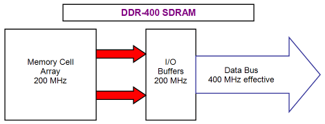 Picture 1. Schematic diagram of data transfer in a DDR-400 chip. Memory chips transfer data to a memory controller via the external data bus on the rising and falling edge of the clock. That's the essence of the Double Data Rate technology. That's why the rating or the effective frequency of DDR memory is always doubled (for example, DDR-400 at 200 MHz data bus). So, the efficient frequency of the DDR-400 data bus is 400 MHz, while its true clock rate (IO buffer frequency) is 200 MHz. Internal clock rate of DDR memory chips (the first generation) equals the true clock rate of the external bus (IO buffer frequency) - 200 MHz for the DDR-400 memory chip. In order to transfer 1 bit per clock (via each data line) along the external bus operating at the effective clock rate of 400 MHz, 2 bits must be transferred per clock of the internal 200 MHz data bus. In other words, we can say that all other things being equal, the internal data bus must be twice as wide as the external data bus. This data access scheme is called 2n-prefetch. 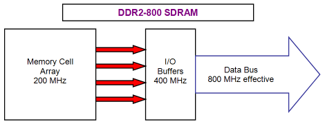 Picture 2. Schematic diagram of data transfer in a DDR2-800 chip. The most natural solution to this problem of obtaining higher clock rates in DDR2 was to reduce the clock rate of the internal data bus to a half relative to the real clock rate of the external data bus (IO buffer frequency). For example, in case of DDR2-800 memory chips (Picture 2), IO buffer frequency is 400 MHz, and the efficient clock rate of the external data bus is 800 MHz (because Double Data Rate is still in force - data are still transferred both on the rising and falling edge of the clock). Clock rate of the internal data bus is just 200 MHz, so in order to transfer 1 bit (via each data line) per clock of the external data bus operating at the efficient clock rate of 800 MHz, 4 bits must be transferred per clock of the internal 200 MHz data bus. In other words, an internal data bus of DDR2 must be four times as wide as its external bus. This data access scheme, implemented in DDR2, is called 4n-prefetch. It has evident advantages over 2n-prefetch in DDR. On one hand, one can use twice as low internal clock rate of memory chips (200 MHz for DDR-400 and just 100 MHz for DDR2-400, which significantly reduces power consumption) to obtain equal peak memory bandwidth. On the other hand, the internal clock rate of DDR and DDR2 memory chips being equal (200 MHz for DDR-400 and DDR2-800), the latter will have twice as high theoretical bandwidth. But its drawbacks are evident as well - DDR2 chips operate at a twice as low clock rate (with the theoretical bandwidth of DDR and DDR2 being equal) and use a more complex 4-1 conversion, which results in noticeably higher latencies. We saw it in practice, when we tested the first samples of DDR2 memory. 4n-prefetch is not the only innovation in DDR2, of course. But it's the most significant difference from the previous generation of memory (DDR), so it's sufficient for our brief review. You may read more details about DDR2 in our article "DDR2 - the forthcoming replacement of DDR. Theoretical basics and the first low-level test results". Further development of the DDR2 technology was similar to the development of its previous generation, DDR memory. Namely, the clock rates reached 333 and 400 MHz (that is DDR2-667 and DDR2-800 official standards). Latencies dropped significantly, there appeared a new official version of JEDEC (JESD79-2B), which allows to reduce timings from 4-4-4 to 3-3-3 for DDR2-533, from 5-5-5 to 4-4-4 for DDR2-667, from 6-6-6 to 5-5-5 or even 4-4-4 for DDR2-800. They were followed by non-standard modifications of DDR2, of course. Their clock rate exceeded the JEDEC bounds - up to 625 MHz ("DDR2-1250") with 5-5-5 timings, or "standard" DDR2-800, but with extremely low timings, for example 3-3-3. As before, such results required a significant rise in memory voltage from standard 1.8V to extreme 2.4V (it's a tad lower than the standard voltage for the previous DDR memory generation - 2.5V). It certainly required more advanced ways to channel the heat away from memory chips - original, patented heatsink designs as well as external active cooling. Nevertheless, as in case with the previous generation of DDR memory, DDR2 technology has almost reached its maximum (in frequency, latencies, and significantly increased heat release owing to much higher voltages). And now we can expect another evolutional leap in the DDR SDRAM technology - DDR3. 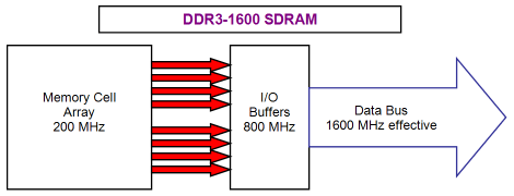 Picture 3. Schematic diagram of data transfer in a DDR3-1600 chip. It's easy to guess that the DDR2-DDR3 upgrade is based on the same principle as the DDR-DDR2 upgrade. Namely, DDR3 is still DDR SDRAM. That is data are still transferred both on the rising and falling edge of the clock at the doubled effective frequency relative to the memory bus clock rate. Only performance ratings have grown twice as high versus DDR2 - typical performance categories of new DDR3 memory will vary from DDR3-800 to DDR3-1600 (and probably higher). The next doubling of theoretical memory bandwidth has again to do with halving of their internal clock rate. That's why in order to reach the data transfer rate of 1 bit per clock along each line of the external data bus operating at the effective frequency of 1600 MHz (as in Picture 3), 200 MHz chips must transfer 8 bits per clock. That is the internal data bus of memory chips will be eight times as wide as their external data bus. This data transfer scheme with "8-1" conversion will evidently be called 8n-prefetch. Advantages of the DDR2-DDR3 upgrade will be the same as in case of the previous DDR-DDR2 upgrade: on one hand, it's a reduction of memory power consumption while preserving peak memory bandwidth (DDR3-800 versus DDR2-800); on the other hand, it's an opportunity to increase memory clock rates and theoretical bandwidth and retain the old level of the internal clock rate (DDR3-1600 versus DDR2-800). Drawbacks will also be the same - a wider gap between the internal and external clock rates of memory buses will result in higher latencies. It's logical to assume that the relative increase in latencies during the DDR2-DDR3 upgrade will be similar to that of the DDR-DDR2 upgrade. Well, let's proceed to a detailed review of the new generation of memory - DDR3, which will replace DDR2 memory. Some facts about DDR3The DDR3 standard is not yet adopted by JEDEC, it will be done by the middle of this year (it will supposedly be called JESD79-3). So the information about DDR3 memory modules published below is only preliminary. Let's start with DDR3 memory chips, which first prototypes were announced back in 2005. Available samples of DDR3 chips are based on the 90 nm process technology. They require 1.5V, which makes a 30% contribution to the reduction of power dissipated by these memory chips compared to DDR2 chips (powered from 1.8V). Total reduction of power consumption versus DDR2 memory chips of the same frequency amounts to 40%, which is especially important for mobile systems. Capacity of components, stipulated by preliminary JEDEC specs, varies from 512 Mbit to 8 Gbit, while typical memory chips today vary from 1 Gbit to 4 Gbit. Theoretical bandwidth of DDR3 chips is twice as high as that of DDR2 chips owing to the above-mentioned 8n-prefetch (versus 4n-prefetch in DDR2). The number of logical banks in DDR3 chips is also doubled to 8 banks versus 4 banks in DDR2. Theoretically, it allows to increase performance of logical bank interleaving and hide latencies that have to do with addressing the same memory row (tRP). DDR3 chips come in FBGA packages, which have a number of improvements compared to DDR2, namely (Picture 4):
 Picture 4. DDR3 and DDR2 pinouts. Let's proceed to the examination of DDR3 memory modules. Like DDR2 modules, they come in the form of a 240-pin PCB (120 contacts at each side of the module). But they are not electrically compatible with DDR2, so they have a different key notch location (see Picture 5a).  Picture 5a. Exterior of typical DDR3 (top) and DDR2 (bottom) memory modules.  Picture 5b. Typical slots on a motherboard (combo) for DDR3 (blue/pink) and DDR2 (green/orange) memory modules. DDR3 memory modules use the fly-by architecture of the command/address/control bus with On-DIMM termination (with a resistor on a memory module). Diagram of this architecture is shown on Picture 6. It improves the quality of signal transmission, which is necessary when components are operating at high frequencies, typical of DDR3 memory and not necessary for DDR2 components. 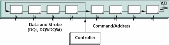 Picture 6. Fly-by architecture of signal transmission in DDR3 memory. The difference between DDR2 and DDR3 (by the example of memory modules, which physical bank comprises eight x8 chips) in address/command/control/clocks is published in Picture 7. Addresses and commands are applied to all chips in a DDR2 memory module in parallel. For example, when data are read, all eight 8-bit data elements will be available at the same moment (after proper commands are issued and corresponding latencies are elapsed), and a memory controller can read all 64 bits simultaneously. At the same time, each chip in a DDR3 memory module receives commands and addresses a tad later than a previous chip owing to the fly-by architecture. So data elements of a given chip will also become available with a certain delay relative to data elements in the previous chip of a physical bank. In this respect, in order to minimize latencies, the new DDR3 memory features a different approach to the interaction between a memory controller and a data bus of a memory module. It's called read/write leveling. It allows a memory controller to use a certain shift in time when it receives/transfers data, which corresponds to the address/command reception delay in a given memory chip. So all data are read (written) simultaneously.  Picture 7. Read/write leveling in DDR3 memory modules. In conclusion, let's analyze speed characteristics of future DDR3 specifications published in Table 1. Table 1. Speed Characteristics of DDR3 Memory Modules
DDR3 memory modules will supposedly come from DDR3-800 to DDR3-1600 inclusive. Then there may appear higher-speed DDR3-1866 modules. DDR3 performance rating takes the form "PC3-X", where X stands for memory bandwidth in a single-channel mode, MB/s (to be more exact - million bytes per second). As DDR3 memory modules have the same bit capacity as DDR2 (64 bits), numerical rating values of equally clocked DDR2 and DDR3 modules match (for example, PC2-6400 for DDR2-800 and PC3-6400 for DDR3-800). Typical timings for DDR3 memory look "impressive" (for example, 9-9-9 for DDR3-1600). But you shouldn't forget that when you convert high relative timings into absolute values (in nanoseconds), they become quite acceptable, considering lower cycle times (as the reciprocal of the memory bus clock rate). For example, CAS# latency (tCL) for DDR3-800 memory modules with 6-6-6 timings is 15 ns, which is a tad too high compared to "typical" DDR2-800 memory with 5-5-5 timings, where tCL is 12.5 ns. And tCL of DDR3-1600 memory with 9-9-9 timings is 11.25 ns - on a par with DDR2-533 with low latencies (3-3-3). Thus, we can expect a gradual reduction of real memory access latencies to typical values of DDR2 memory even in the current situation with expected DDR3 timings. Besides, we shouldn't forget about the further reduction of latencies (and timings) as the technology evolves. Testbed configuration
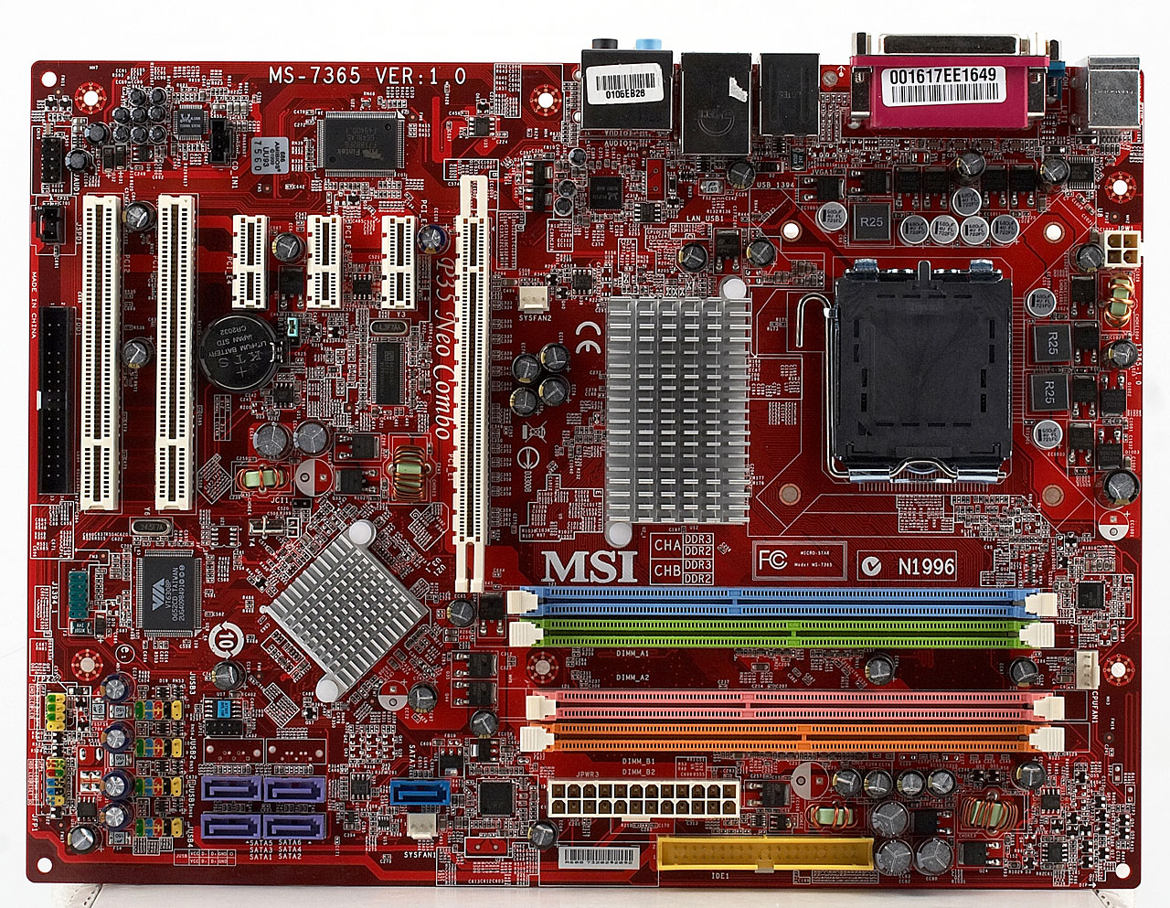 We ran the tests with MSI P35 Neo Combo. The first test resultsLet's proceed from theory to practice. Our testlab got hold of unique pre-production samples of an MSI P35 Neo Combo motherboard based on the new Intel P35 chipset and Corsair XMS3-1066 memory modules (CM3X1024-1066C7 ES). As follows from its name, MSI P35 Neo Combo is a combo motherboard, that is it can accommodate both DDR2 and DDR3 memory modules. Note that the motherboard can use either DDR2 or DDR3. That is simultaneous usage of DDR2 and DDR3 memory is impossible (in the same channel or in different channels). As there is no official specifications on the new chipsets from Intel, we cannot say whether it's a fundamental limitation of Intel P35, or the problem is just in this PCB layout. But the first option is highly probable - Intel chipsets usually do not support such exotic features as using various memory types simultaneously. CM3X1024-1066C7 ES memory modules are engineering samples of DDR3-1066 memory with 7-7-7-21 timings (they match the prospective timings scheme for DDR3 memory modules of this speed group published in Table 1). In order to compare speed characteristics of these memory modules (as representatives of DDR3) with speed characteristics of the current generation of DDR2 memory, we selected Corsair DOMINATOR XMS2-9136C5D modules from the similar speed group (DDR2-1142). We used them in DDR2-1066 mode with nominal 5-5-5-15 timings. DDR2 memory modes and timings were set manually in BIOS, memory voltage was raised to 2.3V. Note that the current BIOS version (V1.0B16 dated 20.04.2007) of the MSI P35 Neo Combo motherboard does not allow to configure DDR3 timings properly. It still offers to adjust main parameters (tCL, tRCD, and tRP) from 3 to 6 inclusive, which corresponds to DDR2 timings, not DDR3. The same concerns memory voltage - you can still control it from 1.8V to 2.5V, while the official DDR3 memory voltage is just 1.5V. That's why we set DDR3 memory settings "by SPD" at minimal 1.8V. But we cannot really say anything about these settings (about real support for the unconfirmed SPD standard for DDR3 as well as correct DDR3 timings for the memory controller in the Intel P35 chipset). We can say only one relevant thing: our combination of DDR3 Corsair XMS3-1066 memory modules and MSI P35 Neo Combo motherboard really works. So let's analyze test results obtained in the latest RightMark Memory Analyzer 3.72, which includes RightMark Multi-Threaded Memory Test 1.0. We'll start with the tests of real memory bandwidth for single-core memory access. As usual, we measured real memory bandwidth in four modes: Read, Write, Read with software prefetch and an optimal prefetch distance, which is 1024 bytes for Intel Core 2 Duo (Read SW PF), and Write NT. The first two modes help us evaluate the average real memory bandwidth for reading and writing. The last two modes evaluate maximum real memory bandwidth for the same operations. Picture 8. Real bandwidth of DDR2 and DDR3 memory, single-core access. Diagram 8 with test results of DDR2-1066 and DDR3-1066 in a single-thread mode shows that DDR3 is outperformed by equally-clocked DDR2 only insignificantly: the difference amounts to 5-8%, it's especially noticeable in maximum real memory read bandwidth. In both cases, the real memory bandwidth values are very far from maximum theoretical bandwidth of DDR2/DDR3-1066 (17.1 GB/s in dual-channel mode). However, it can be easily explained by the following bottleneck - 266 MHz FSB (1066 MHz Quad-Pumped bus), which peak bandwidth is just 8.53 GB/s. Picture 9. Real bandwidth of DDR2 and DDR3 memory, dual-core access. Dual-core memory access mode (both CPU cores access memory simultaneously, Picture 9) allows to reach higher memory bandwidth (about 8.0 GB/s, which is closer to the maximum theoretical bandwidth of FSB - 8.53 GB/s). In this case DDR3-1066 is generally on a par with DDR2-1066. And its maximum real memory read bandwidth is even higher by 2% . Here is our conclusion: what concerns real bandwidth, DDR3 is at least no worse than DDR2 memory of the same frequency on the current generation of Intel platforms, sometimes it's even faster. That is the fly-by architecture for addressing and commands, and read/write leveling, necessary to reach high memory clock rates justify themselves, because they do not make memory performance worse (they may even improve it). An attentive reader may object to these conclusions based on memory tests in dual-channel mode only. Indeed, in this case the bottleneck is not in the memory bus (from two channels of the controller to each memory module), but in FSB (from a CPU to a chipset/memory controller). So can we just fail "to see" the difference between DDR2 and DDR3 for this very reason? As this objection would have been appropriate, we decided to check our conclusion by analyzing results of a single-channel memory mode. This operating mode is of purely theoretical interest these days. But it allows to equate peak bandwidth of FSB and memory bus, and thus eliminate possible effects of the former on low level test results. These results are published in Table 2. Table 2. Real DDR2 and DDR3 bandwidth in the single-channel mode
Both single- and dual-core memory bandwidth values in single-channel mode are expectedly noticeably lower than bandwidth values obtained in dual-channel mode. Moreover, a single-core access mode demonstrates a larger but still irrelevant gap between DDR3 (slower) and DDR2 (4-11%). But the dual-core memory access again equates results of DDR2 and DDR3, and allows the latter to outperform equally-clocked DDR2 by 1-2% in reading operations. Maximum real memory bandwidth of DDR2-1066 and DDR3-1066 reaches 82-83% of their theoretical maximum in single-channel mode, which seems a good result. Test results of DDR2 and DDR3 memory in single-channel mode confirm our conclusions about speed characteristics of DDR3 memory. Well, now we can only evaluate access latencies of equally-clocked DDR2 and DDR3 memory modules. Out of general considerations, we should expect higher values for the latter (considering higher timings - 7-7-7 versus 5-5-5 for DDR2). But we'll see what the real difference in latencies will be. Note that in this case we obtained practically identical results in dual-channel and single-channel modes, so we'll publish results for dual-channel mode only (see Picture 10). Picture 10. DDR2 and DDR3 memory latency. So, DDR3-1066 latencies are naturally higher than those of DDR2-1066. The relative latency growth is 13% for pseudo-random access and 16% for random access. Nevertheless, if we take into account that the difference between 7-7-7-21 and 5-5-5-15 is good 40% (as we have written above, we cannot say anything certain about real DDR3 timings), the real increase in latencies looks more than acceptable, when we upgrade from DDR2 to DDR3. ConclusionsResults of our first low-level tests of DDR3 engineering samples in comparison with equally-clocked DDR2 memory modules in identical conditions allow us to conclude that memory of the new DDR3 standard (still unadopted) is justified even today. Its speed characteristics are at least no worse than those of DDR2 memory modules, sometimes they are even better. The relative DDR2-DDR3 latency growth is not high either (13-16%), all other things being equal. And if we take into account that development of memory technologies generally follows the trail of simultaneous growth of clock rates and reduction of latencies, the future generation of DDR3 memory can close in this gap, or even outscore DDR2 in latencies (DDR2 has practically stopped its development now). At the same time, we should note that DDR3 will have the same lot as the current generation of high-speed DDR2 memory (DDR2-800 and higher). Namely - serious problems with revealing the huge performance potential of this memory type, which stopped being a bottleneck long ago. For example, our Intel Core 2 Duo / Intel P35 platform can reveal the potential of DDR2-1066 or DDR3-1066 only in the single-channel mode (the real memory bandwidth in this case reaches 83% of the theoretical maximum), which is of no interest from the practical point of view. And the dual-channel mode seriously restricts memory bandwidth on the side of FSB, which bandwidth is twice as narrow. We mentioned such limitations in our articles about system memory (see, for example, Digest 2006). We can only hope that manufacturers of the most important PC components - processors and chipsets - will see the need to modernize their products to reach high performance standards dictated by... memory technologies. MSI P35 Neo Combo kindly provided by
MSI Russia Corsair XMS3-1066C7 memory modules kindly provided by Corsair Memory Russia Dmitri Besedin (dmitri_b@ixbt.com) June 29, 2007 Write a comment below. No registration needed!
|
Platform · Video · Multimedia · Mobile · Other || About us & Privacy policy · Twitter · Facebook Copyright © Byrds Research & Publishing, Ltd., 1997–2011. All rights reserved. | ||||||||||||||||||||||||||||||||||||||||||||||||||||||||||||||||||||||||||||||||||||||||||||||||||||||


