 |
||
|
||
| ||
|
||
|
||
| ||
A week has not yet passed since the previous article was published about power consumption management technologies in modern processors, but our test lab already got hold of Intel Pentium 4 processor, and a week later – Intel Xeon with a new revision of Prescott and Nocona cores (E0 stepping, CPUID = 0F41h signature). The former demonstrated seemingly interesting behaviour in the halt mode (it will be described below). We have found out the reason soon enough – it turned out that the new revision of Prescott core supports the new Enhanced Halt State (aka C1E) technology together with Execute Disable (XD bit) and Thermal Monitor 2 (TM2). A similar operating mode and the Enhanced SpeedStep (DBS) technology for servers are also implemented in the new revision of Nocona core. The present article is devoted to the C1E technology analysis as well as to Thermal monitoring mechanism #2, which is implemented in Pentium 4/Xeon processors in new Prescott/Nocona core revisions. Testbed configurationsTestbed 1
Testbed 2
Software
Enhanced Halt State technology
According to the available documentation, Enhanced Halt State (C1E) is an operating mode of a physical processor with low power consumption, which is activated when both logical processors go to sleep (the HLT or MWAIT instruction) if this technology is enabled in BIOS. So what's the difference between this low power mode and the "usual" Halt State (C1)? In this case a processor can dynamically reduce the motherboard frequency multiplier (FID) and voltage (VID) and restore to maximum performance state (nominal FID/VID) when necessary. This can be done absolutely automatically (without operating system interference). One can say that C1E is a compromise between the old ODCM technology, which automatically decreases effective CPU clock by modulating it in the halt state as demonstrated, and the new server Enhanced SpeedStep (DBS) technology, which can change the effective CPU clock and voltage, but does it "on demand" instead of doing it automatically.
Well, it's time to see the new technology in action. For this purpose we'll use RMClock, which has obtained additional features since the previous article. In particular, it has specific settings for power management functions in Intel Pentium 4, Xeon and Pentium M processors, so that we can now do without extra utilities, such as CPUMSR.

But we have to precede the discussion of results with one important qualification – the processor in our test lab turned out an engineering sample (as reported by Intel Processor ID Utility). In this connection we can expect that the behaviour of production samples may differ from that demonstrated by our processor in today's tests.
 The second important issue – C1E detection is implemented in the hit-and-miss fashion so far. Thus it is of a presumptive character (nevertheless, it functionality is field-proven).  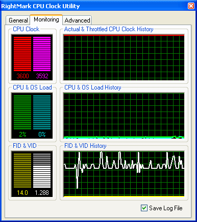
Let's proceed to the main tabbed pages of the application – that's how they look in a couple of minutes of operation when the CPU is not loaded. On the left picture you can see that the processor supports TM1, TM2, ODCM and C1E. Only TM2 and C1E are currently enabled (i.e. by default). The C1E effect is already noticeable – just compare the current FID and VID values of the processor with the nominal ones. The first one is at minimum, the second is somewhere between minimum and maximum. You can see the FID/VID history on the right picture – at minimum CPU load, FID remains on the constantly low level (14x), VID varies within a wide range, its average value being about 60% of the nominal one. In fact, VID changes may fail to reflect the real changes of CPU voltage, because VID is just a voltage value requested by a processor, but a motherboard is actually free to do anything with this request (change nothing, first of all). Nevertheless, we monitored real CPU voltage changes in our tests as well (using Hardware Monitor from Intel Desktop Utilities, which relies on readings of motherboard sensors). It was approximately 0.1V lower than VID values.
 So, everything is great with FID and VID, however we cannot miss another important issue – CPU clock as such. Both the actual CPU clock (measured by TSC) and the throttled CPU clock sort of remain... at the constantly high level. To be more exact, the throttled CPU clock is within 3590...3600 MHz, which is just 10 MHz lower than the nominal clock. There is actually nothing surprising in this seemingly unusual phenomenon. Considering the C1E nature (it's activated only when both logical processors go into the C1/HALT state), there is absolutely no opportunity to see it in action. Because even the most precise methods for measuring CPU clock will inevitably make a processor switch from sleep mode (C1) into operating mode (C0), which restores full CPU clock. Let's try to disable C1E on the CPU settings tabbed page.  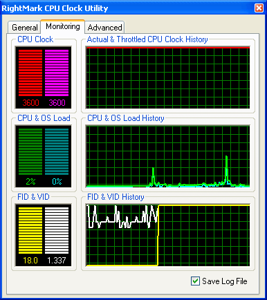 The result is illustrative – disabled C1E immediately results in maximum FID and VID set as defaults. After that they are kept at the constant level irregardless of the CPU load. And the effective CPU clock becomes stable at the level of its actual (nominal) clock – 3600 MHz.
The next experiment – we restore C1E and apply variable load to the processor, imitated by a simple simulator.
 FID/VID curves prove that the processor can switch fast between minimal/maximal P-State Profiles. To all appearances there are only two FID states (initial and final), while VID changes may undergo many intermediate states (at 0.0125 V steps). Thus, the Enhanced Halt State technology is quite a promising innovation, which reduces the power consumed by a processor in the halt state much more effectively compared to the regular C1 mode (HALT). The introduction of this technology may raise a question: if there is a completely automatic C1E (which is also used in new Xeon Nocona processors, by the way), why do we need Enhanced SpeedStep for servers (DBS), which requires "manual" (program) control? The answer to this question is very simple: C1E is really a completely automatic technology, it can reduce power consumption of a processor only at full system halt and restore the system to full performance at the least CPU load. And DBS can force down the power consumption of a processor in normal operation, including considerable system load (if the controlling software decides that there is no need in full capacity of the server). Automatic thermal monitoring mechanism #2Attentive readers may have noticed: the Thermal Monitor 2 technology was already reviewed in the previous article, why review it again here? The answer to this question will be simple and unexpected – after the tests we found out that in fact the reviewed model of Xeon Nocona (D0 stepping, CPUID signature – 0F34h) did not support TM2! To be more exact: "TM2 is enabled, but NOT supported". It is really enabled – this technology is indicated in CPUID Feature Flags. And according to the test results, it works fine. But at the same time it's "not supported"... So we decided to examine this technology using a processor (not a production sample, though), which supports it officially.
The research technique will be absolutely the same: 100% load applied to both logical processors and a stopped fan in the CPU cooler.
 The result is quite expectable (and the picture is similar to the one we obtained with a Xeon processor) – when a processor reaches 73°C, the effective CPU clock decreases together with CPU load. The FID/VID graph demonstrates FID fluctuations between the two levels – minimum and maximum. At the same time you can see that VID can be switched via intermediate states (as in C1E, only the changes are more abrupt). TM2 starts to work at its full in about a minute after the fan is stopped. The effective CPU clock reaches 2.8 GHz, the CPU load stops at 77.7%, and FID/VID stop at the level of target values (TM2 Target FID/VID) 14x and 1.2V correspondingly. Active CPU cooling restoration results in the same changes mentioned above, just in the reverse order. DiagramTo get a complete picture, we ran a third party utility ThrottleWatch and repeated this test (when it was released, we already had no opportunity to test its operation in TM2 mode). The result is obvious – ThrottleWatch can detect and track the moment when the system enters/leaves TM2. However, its functionality in other CPU throttling modes is still dubious. New revision of Nocona core in Intel Xeon processors
And finally, let's review a similar E0 revision (CPUID = 0F41h) of Nocona core in Intel Xeon 3.6 GHz processors. At first we'll study which of the reviewed power management technologies are available and enabled by default in this group of processors. 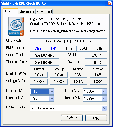 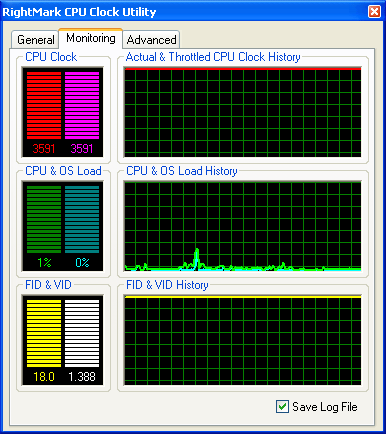 So, the new revision of Nocona core supports all five "thermal" technologies – from "ancient" ODCM and TM1 to the new TM2, DBS, and C1E. The following technologies are enabled at startup – DBS (by the way, you can enable/disable the Enhanced SpeedStep for servers in BIOS settings; besides, it's automatically enabled by RMClock at startup) and, strange as it may seem, the old modification of thermal throttling – automatic thermal monitoring mechanism #1 (TM1), unlike the 3.6 GHz Pentium 4. Interestingly, BIOS sets target FID/VID for TM2 correctly (you can see that by Minimal FID/VID), but for some reason this technology is not enabled by default. And finally, C1E is also disabled by default (it can be enabled/disabled in BIOS), which is clearly demonstrated on the right screenshot: FID/VID values do not change in time. One can assume that disabled C1E on a server platform is dictated by maximum performance issues (minimum server response time to requests): both entering C1E and leaving it are accompanied with larger delays compared to entering/leaving the regular C1 (HALT) state, due to necessary switching between CPU operating modes (FID/VID) to lesser power consumption and back. No matter what manufacturers of processors, chipsets, and motherboards do with their products, we can always enable necessary options manually, using the Advanced tabbed page in RMClock. Let's enable TM2 (actually we could have left it disabled), C1E, and see the results. 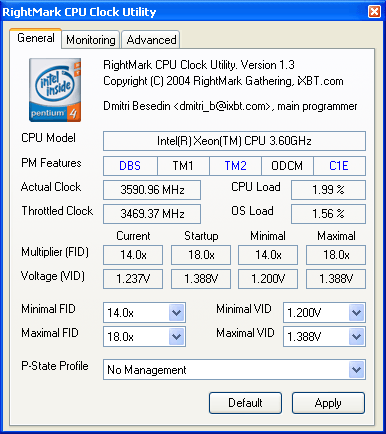 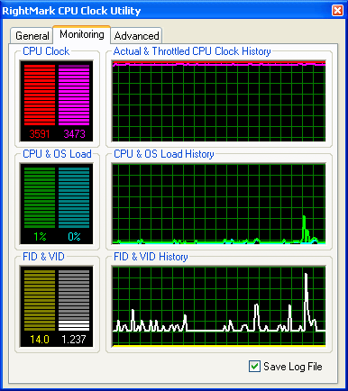 C1E in action. CPU multiplier dropped to the minimum 14x (that is according to our working hypothesis, the CPU clock was modulated with 77.7% duty cycle), the core voltage started to "jump" between minimum and maximum, being mostly at 1.237V. The effective CPU clock went down, its minimum level being at about 3470 MHz. So, C1E in Xeon (Nocona) processors works correctly.
And now let's see how the two latest functions of controlling CPU operating modes (Enhanced SpeedStep (DBS) for servers and Enhanced Halt State (C1E)) work together. These days such a situation can be demonstrated only by the latest Intel Xeon processors. Let's set the minimum FID/VID to 14x and 1.2V correspondingly and then use RMClock to set P-State Profile to Minimal.

Here are the results: the effective clock is reduced to ~2.8 GHz, FID/VID – to the requested 14x and 1.2V. C1E technology is sort of disabled – effective CPU clock as well as its voltage cannot be any lower. Let's proceed: set the P-State Profile of the processor to Maximal (FID = 18x, VID = 1.388V).

The processor demonstrates curious behaviour in this mode: C1E obviously "prevails" over Enhanced SpeedStep despite the forced maximal FID/VID – the effective CPU clock goes down, FID and VID oscillate between the minimal and maximal levels. That is now DBS is "sort of disabled", not C1E. Another experiment: we'll retain the Maximal P-State Profile, but... the voltage will be reduced to minimum (this is quite possible, when a CPU is not loaded), that is FID/VID will be set to 18x and 1.2V.
 Now C1E is really disabled, complete control is passed to DBS. So we can draw an interesting conclusion: to make the C1E technology possible, CPU voltage (VID) must differ from the minimum possible voltage (set in TM2 Target VID) at least by 0.0125V. In other words, first of all various CPU performance/power consumption states mean VID values for C1E, while FID values are secondary. Summing it all up
Our previous article started and the present one finished the review of modern performance and power management technologies in Intel Pentium 4 (Prescott) and Intel Xeon (Nocona). The main conclusion has been already made – all the technologies reviewed, from the first ODCM to the latest Enhanced SpeedStep (DBS) and Enhanced Halt State (C1E) seem to be based on a common idea – CPU clock modulation (duty cycle). It may seem "unfair", cheating consumers. That's not the case, of course. We have never said that. In fact, it's just one of possible (and the simplest) ways to implement these technologies, but it's no less effective than "more honest" ways. Besides, don't forget that it's one of possible opinions (of the author), with which you may just as well disagree. You can think of an alternative opinion, much more "correct" according to the official Intel's documentation. But what is a possible alternative? Considering that some processor units (e.g. bus arbiters, asynchronous prefetchers, etc) most likely cannot easily switch between various performance modes, one can assume that Intel engineers most likely "divided" the processor core into several individually clocked components (due to several PLL, or due to prescalers transforming the reference clock). Some of these components always operate at full clock (including Time Stamp Counter, its readings are used in the conventional method for measuring CPU clock), while the other components (executive modules) can operate at lower clocks. It's not quite clear though why Intel engineers decided that TSC should operate at full clock, while Performance Monitoring Counters (PMC) operate at "reduced" clock? Possible explanations of this fact as well as the choice between the above mentioned opinions are up to our readers. What concerns us, we didn't find any experimental evidence of the second, more "official" hypothesis in the course of our research. Of course, we have no obvious evidence of our point of view, except for the fact that it does not contradict the experimental facts. So let's apply the rule of contraries. The main contradictions to our opinion are (1) the incorrect CPU clock measuring technique and (2) our announcement that Pentium 4 and Xeon processors can operate at full clock at reduced voltage (in TM2, DBS and C1E modes).
Let's start with the first contradiction. There is no doubt that the actual CPU clock is measured correctly – this method is used by all system utilities (CPU-Z, WCPUID) without exception, the operating system itself, as well as... by Intel Processor Identification Utility! The screenshot below is taken on an Intel Xeon 3.6 GHz processor with enabled Enhanced SpeedStep.
 In our opinion, no comments are necessary: CPU clock is measured by TSC (3.6 GHz), and the FSB clock is measured by dividing it by the current 14x multiplier, which results in the wrong value of 1028 MHz and an illustrative label "Overclocked!". So, if the "wrong" method is used by Intel's utilities as well, what is a "correct" method then? Such formulas as FSB_freq = TSC_freq / Startup_FID i.e. multiplying the FSB clock by the current multiplier? (to all appearances this method was used to demonstrate DBS at IDF 2004 Russia) Sorry, this is not measuring but mere adjusting, wishful thinking. Besides, it obviously cannot be an all-purpose method, that is it will not be good for any x86-compatible processor. Now what concerns the second statement. At first sight it looks evident: reduced CPU voltage (when TM2 snaps into action with enabled Enhanced SpeedStep and Enhanced Halt State) must result in the reduced actual CPU clock. But that's only the first impression – the facts speak of the contrary. First of all, have a look at the last screenshot in the previous chapter – you will clearly see that the Intel Xeon 3.6 GHz processor can operate at full clock (FID = 18x) at quite a low voltage – 1.2V (0.1875V lower than nominal!). And secondly, let's carry out another interesting experiment – take an unlocked Intel Pentium 4 560J (Prescott) 3.6 GHz processor and make it think that it operates at the minimal clock (FID = 14x), but... raise the FSB clock to 266 MHz (we described this procedure in detail in the article "Unveiling DDR2-533 Potential. Part 2: 266 MHz FSB, Intel Pentium 4 Prescott processor").  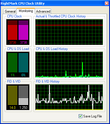 Look what happens: the processor is sure that it still operates in standard mode; so it controls its voltage dynamically in the halt state using the C1E technology. But its real clock (both actual and effective) is equal to 3.74 GHz. So, Pentium 4 and Xeon processors can actually operate at full clock at reduced voltage, if they are in the halt state (C1/C1E). Thus, the facts mentioned above don't corroborate, but just support our conclusion that the performance and power management functions in Intel Pentium 4 and Xeon processors have the same basis. Write a comment below. No registration needed!
|
Platform · Video · Multimedia · Mobile · Other || About us & Privacy policy · Twitter · Facebook Copyright © Byrds Research & Publishing, Ltd., 1997–2011. All rights reserved. |


