 |
||
|
||
| ||
|
||
|
||
| ||
Modern PDAs and smartphones have very strict requirements for the elemental base - you can come across models which are 1 cm thick and weigh 100 g in spite of their iron case, capacious batteries and a big screen. Looking at my HP iPaq 1910 I wonder whether there's a board with a processor, memory and other logical elements at all: How did they fit it in there? Such miniature dimensions are possible due to the compact systems which house not only the CPU core but also many other controllers such as controllers of an LCD screen, power supply and core clock management, USB, audio interface, interfaces of memory cards of various standards and general I/O interfaces (for buttons, wheels and joysticks). The chip also integrates a controller of various system memory types, both random-access and Flash. The latest solutions are even more integrated: the chip based system also contains one or two Flash dies for OS and other software. Soon it will also integrate RAM of the industry standard size: 32, 64 and 128 MB. Today we'll get into the history, look at the prospects and the current situation of the most popular chip based systems - Intel's PXA products based on XScale's RISC core. A bit of historyThe Intel XScale RISC originates from a very successful solution from Advanced RISC Machines Ltd (of the RISC architecture named ARM) and is the extension of this architecture being backward compatible in software. ARM was founded in 1990 by Acron, Apple (sic!) and VLSI. Acron wanted a CPU for its Archimedus PC, which had a successful architecture but failed to become popular. Apple looked for a RISC architecture to replace MACs based on the Motorolla 68k CISC architecture, and VLSI planned to make processors based on this architecture to use it in various integrated and flexible systems. The architecture turned out to be a success: various ARM core versions (especially 6,7,9,10,11) and various finished solutions were licensed for a wide range of companies including DEC, Intel, TI, Atmel etc. The solutions had low power consumption (relative to the performance) and flexible adaptation for specific needs including additional instructions sets for signal processing (multimedia) or effective implementation of Java byte code. Here are some of ARM solutions: 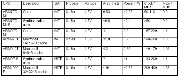 Here you can find details on the basic architecture, instructions and other aspects of original ARMs. This simple and easily adaptable architecture pressed out its competitors from the PDA market (other popular RISC architectures NEC VR and MIPS) and the Motorolla DragonBall that descends from single-chip Motorolla 68 microcomputers. At the moment the ARM architecture and its derivatives serve a base for most chip based mobile solutions from various manufacturers (not only from Intel, but also from Atmel and Texas Instruments, like OMAP and others). Three most popular (in such devices) mobile OS core - Windows CE, Symbian and PalmOS - have been developing within the frames of this architecture. Linux solutions which are much less popular are also ported to the ARM. This architecture reigns on the market of PDAs, smartphones and other smart mobile solutions. The periods of domination of this architecture (in one or another Hi-tech sphere) alternate with the periods of competition of several architectures. In different spheres such alternation has different speeds and time of "monarchy and democracy". x86 architectures have been reigning on the PC market for a long time already (except for the PowerPC in Apple's products). I think that the ARM's domination in some or others forms on the market of PDAs and smartphones won't end soon. The matter is that what PDA designers prefer doesn't depend on development of the architecture - the computational power is important but it isn't determining. Simplicity, low power consumption, flexibility, software and development tools are the most important, and the ARM architecture has no problems with it. A lot also depends on how the system is realized on the chip, what controllers and subsystems are integrated, what memory types and size are supported, how much power is consumed etc. But all such aspects develop independently from the core architecture. By the way, in a modern system of such class the core takes less than half of a die, the other part is taken for controllers and other service systems. A bit after the announcement of the ARM, DEC licensed the ARM architecture and instruction set and developed their own advanced version of the core named StrongARM. When DEC merged with Compaq, the StrongARM core was purchased by Intel, and then for a long time it served a base for SA1110 based systems for Windows CE PDAs. The integration degree in such systems was lower compared to modern solutions, and many functions were on the shoulders of the second chip-companion. They had a dated serial interface and some other features which are not used anymore. Then Intel developed its own core and architecture version compatible with the ARM v5 in instructions - Xscale. The new core consumes less power and scales better as the core clock grows up - 400MHz solutions are already available and 600/800MHz versions based on the Xscale are expected soon. Besides, the new architecture supports instructions that deliver effective communication with various coprocessors based on the same chip. One of the main extensions is the Wireless MMX, a 64bit SIMD instruction set and a SIMD coprocessor which will be integrated into new XScale based chips. These instructions effectively process video, 3D graphics, sound and other elements traditional of SIMD. Although this set is not compatible with the SSE/SSE2 of Intel's desktop solutions, it has very similar features, that is why algorithms are not needed to be rewritten, vector commands can be translated without any changes in many cases, only the precision and data representation must be controlled. For effective utilization of software on Xscale based systems they should be recompiled with an adequate optimizing compiler to let the performance grow twice. In this respect the situation reminds the release of the Pentium - software compilation was oriented towards the 486 processors and the programs ran not very efficiently, but later, with appropriate compilers the performance grew up considerably. FamilySo, the Xscale core is used for all Intel's systems produced for PDAs, smartphones and other mobile applications. Intel PXA255
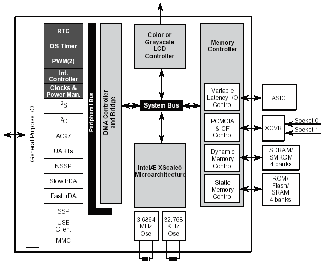 This is a block diagram of the PXA256. The configurable memory controller on the right also executes functions of the CF/PCMCIA interface. Up to 6 banks can be configured, each can be CF/PCMCIA, RAM or ROM, with different parameters and memory bandwidth. The left part is provided for controllers of various devices, some of them have a direct access to data, via a DMA channel, taking them from the system memory. Here are they:
The system also contains the display controller supporting 1,2,4,8 and 16 bit color (up to 8 bits per color and 16 bit palette), active and passive matrixes supported, with one or two pages. The maximum pixel frequency is 83 MHz. For example, for the display of 800x600 at the refresh rate of 75 Hz the pixel frequency must be 36 MHz. The maximum resolution supported is 1024x1024. The quality hardware 16-bit dithering is realized for passive panels. Intel PXA26XThe main advantage and distinguishing feature of this model is the Flash memory integrated into the same package. Such integration degree makes this solution attractive for smartphones and usual cell phones with advanced functions. Here's the cross section of this chip based system: 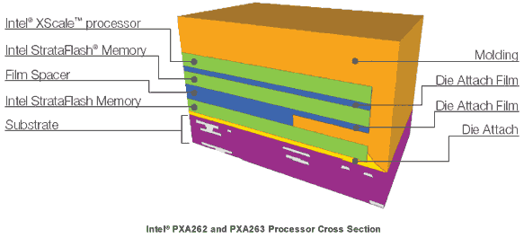 One processor die and one or two Flash memory dies. Besides, the new series has more peripheral controllers. So:
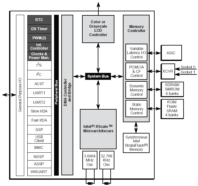 So, the main difference between the block diagrams of the PXA26x and PXA255 is the synchronous Flash memory and additional controllers. The onboard Flash memory takes one of 6 banks, and the solution with the 256MB DRAM will have only one free bank for the CF/PCMCIA slot or other equipment of this kind (so called Variably Latency I/O Control). NSSP and ASSP indicate I/O interfaces meant for mobile (cellular ) applications - Network and Audio interfaces respectively. Now let's see what's the use of such thick integration of functions and controllers in one chip. Here is how AC97 codecs are connected - one or even two: 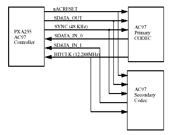 And this is the display connection scheme: 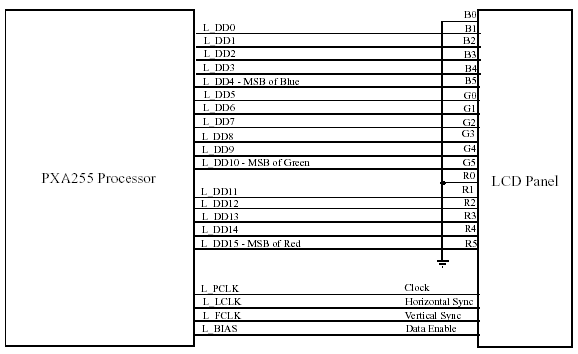 And this scheme is for the MMC memory card connector (they couldn't avoid using several resistors): 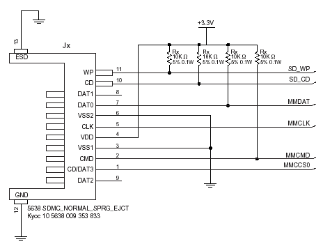 About 90% of devices and schemes of a modern PDA or smartphone connect directly to its heart, the chip based system, without any intermediaries or unnecessary components. This is what the high system integration degree means. FutureWhat should we wait from such systems in future (in chronological order)?
The integration degree is growing up. Why to solder unnecessary chips to the board? An ideal system must remind my old digital organizer, i.e. a board with one chip, battery, screen and pins for buttons. And what about connectors? Are they really needed in the epoch of wireless peripheral interfaces? All in chip... The only connector you have to bear is the power supply one. ;-)
Alexander Medvedev (unclesam@ixbt.com)
Write a comment below. No registration needed!
|
Platform · Video · Multimedia · Mobile · Other || About us & Privacy policy · Twitter · Facebook Copyright © Byrds Research & Publishing, Ltd., 1997–2011. All rights reserved. |


