 |
||
|
||
| ||
|
||
|
||
| ||
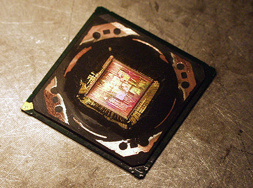 Today we will make a virtual trip into insides of NVIDIA's Californian office. The company is headquartered in Santa Clara, pretty close (15-20 minutes by car if there are no jams) from the established business and cultural center - San Jose. Three large beautiful buildings (it takes ten minutes to go around them) hide an inner yard where you can get only from the office territory. So, we are in the main hall where one must pass the registration procedure to get inside (like in any decent operating system or Windows XP): 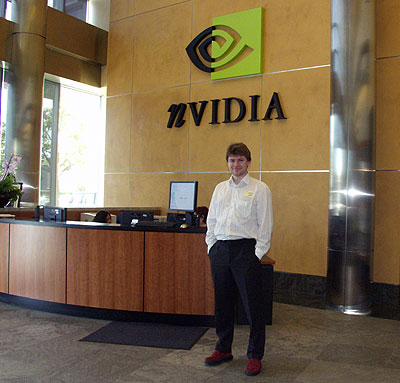 The guy you can see above will be your guide in this virtual trip; it's me :-) Also you can see a big LCD display there with Sign In application where every visitor must enter his or her name, their company's name, a person he/she visits and accept the licence agreement. It's like being inside a software product :-) Then they give you a disposable badge which you can stick to your shirt. We can start our trip from admiring various awards and prizes received from NVIDIA's partners and mass media. But we'll skip these numerous bells and whistles and go directly to the holy of holies - NVIDIA's labs and premises. In general, the building looks integral and unobtrusive; a peculiar style, dimmed light and no noise:  Beautiful topping and wide stairs look so familiar:  Black, yellow-rimmed roundish metallic pimples on the stairs. Oh, yes! It's the first Unreal - one of the space ships had this kind of ramps and stairs. How funny! But the stairs are not the major pride of the headquarters. There is also a cafe, a bit later we'll pop in there for a bite, and now let's move on to the server room:  Company's Heart. Should anything happen there, and the company's performance will immediately slump down. The room is huge - there are 5 rows of mounts over 25 m long and some free space. They all are droning, buzzing and blow air at you: 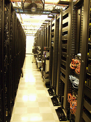 Are you again caught in the cables? Be careful...  This is Joseph ("Server Guy") - father of NVIDIA's multiple clusters, disc arrays and servers: 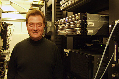 Next to him are various auxiliary servers controlling e-mail, internal databases which are not directly connected with chip development, distributed bug-lists and other tools used for a myriad of day-to-day company's needs:  Here they store various service databases and work files. Impressive? And what about the woolen nap of cables on the left? These red boxes  house NVIDIA.COM. The actual IP address is blackened for protection. As you can see, beside 1Gbit Ethernet they use optical connection. It's not simple to physically commute all this stuff 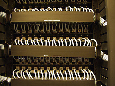 For logic protection and routing they use mostly Cisco's solutions of average and high power. 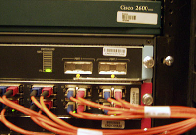 Basic pathways connecting servers and disc arrays (server file) are optical. Now, my dear tourists, when you've got an idea on how powerful these capacities are, let's see how and what for they are used. Chips are developed the following way. It starts with preliminary scientific, algorithmic and architectural researches in order to develop new algorithms and approaches to realization. This a continuous process parallel to creation of other certain products and it can involve several projects. Many people at NVIDIA can make researches apart from their primary activity related with product development and debugging. Besides, some researches, like in hardware real-time computer graphics, are carried out outside the company, for example, in Stanford. Then a chip architecture is formally described in a special language similar to popular programming languages and meant for formal description of hardware incarnations of some or other algorithms. Such approach defines intermodule interfaces and divides the chip into separate tasks (blocks) which are then independently elaborated. It makes the procedure simpler and faster and allows using finished blocks of different levels repeatedly (from petty utilitarian ones to whole processors such as vertex and pixel pipelines). Verilog and VHDL are the most widespread languages of this type (so called HDL languages). It takes up to 4 or 5 months to make up a software description of a chip depending on how much is taken from previous projects. Then the description is tested and debugged in software simulators which run HDL programs. The process takes the most part of computational resources. The stages can involve separate units (then they are processed simultaneously with the previous stage) or the whole description. HDL simulation tasks can be perfectly paralleled and take little time - as a rule, several hours for one task, 24 hours at most. But the number of tasks is so great that it's necessary to provide clusters of thousands of processors to provide acceptable response time, and, therefore, acceptable time of chip development. There are two emulation levels: interpretation of the original description and generation of logical topology (i.e. representation on the level of transistors and links between them) for a program defining chip architecture. You can call it basic logic compilation. A big LINUS cluster based on x86 processors is used for tasks of HDL compilation and simulation:  front view  back view 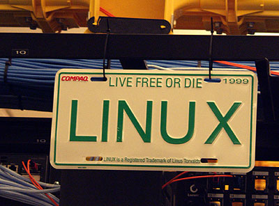 These servers are mostly dual-processor Pentium IIIs based solutions, though earlier they were composed of Celerons but some time ago these CPUs were replaced. Some of the servers are uni-processor solutions. Half a year ago Pentium IIIs had the best price/perfoprmance ratio for HDL tasks but now it's different. A bit later we will get back to it. When development and debugging of an HDL model is finished there comes the final compilation and optimization of the logical topology. The obtained logic model is tested on hardware logic simulators with flexibly programmable connections, for example, for this purpose NVIDIA uses red boxes from IKOS - FPGA (Field Programmable Gate Array) for chip hardware emulation. Such emulators are relatively inexpensive - the price is around $10,000; and it's much more advantageous to tune all tasks with them than to use real chips which require half a million of investments and a month to get the results. The simulators can be connected to real computers which run real applications though the speed can be thousands of times lower as compared to normal GPUs. So, chips can be tested on real programs yet before they are physically created. The next stage is to arrange chip's physical topology. It requires much time (dozens of days) and involves trying and optimizing various topological structures in volume (huge RAM size, 64bit memory addressing is obligatory!) regarding tough rules based on the clock speed and various topological norms. As large zones of the chip are processed as a whole, it's almost impossible to parallel such task for an inexpensive cluster comprised of unsophisticated computers. Another aspect is reliability. A cluster consisting of a large number of x86 processors is guaranteed to work flawlessly several days only; it's not enough for arranging chip's topology. This stage is followed by taping out, i.e. passing the information to the factory where first templates are made and then first chips are brought out. For this purpose NVIDIA uses very expensive Sun's 64bit platforms:  Each of 11 such units, 2 m high, works independently, costs $1,000,000, contains from 32 to 96 processors and 192 GB memory (each). NVIDIA has been looking for a substitute for such expensive (in particular, in operation) solutions for a long time already. One of the solutions can be Itanium based clusters - Joseph was looking forward to first IBM models Maddison on Itanium 2. The preliminary tests carried out on already available Itanium 2 models, not less efficient, proved that clusters made of relatively inexpensive 2- and 4-processor servers can be perfectly used for HDL tasks, and servers made of more processors can finally replace Sun's solutions. The question is in reliability and memory size of fast 64bit addressing. The computing factory is vital for NVIDIA. These computers, speaking jokingly, develop chips all days long instead of people who get their salaries for making mistakes and then looking for them :-) That is why increasing of computer power is a foreground task. NVIDIA keeps on buying small lots of inexpensive servers on x86 or Sun platform, test them and decide whether to buy bigger lots. Another problem is how to supply power and cool all these silicon heaters. Look: they have huge droning digitally controlled stands next to:  These are emergency power supply units. Blowing out of fuses is not a rare thing when thousands of processors work in parallel. Nobody wants to lose data of a month's simulation. Young man, what are you doing?! Don't press the red button!!! The second server room is also filling with the units bit by bit; it is located in another building due to problems with power supply and power consumption. Let's go there through the yard,  admiring recently planted blooming sakuras (it's spring indeed!) 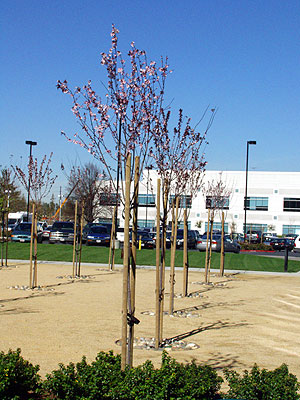 The people over there have a nice talk being caressed by the shiny sun but one queer guy  seems to be reading some associated documentation  [ Second Page ]
Alexander Medvedev (unclesam@ixbt.com)
Write a comment below. No registration needed!
|
Platform · Video · Multimedia · Mobile · Other || About us & Privacy policy · Twitter · Facebook Copyright © Byrds Research & Publishing, Ltd., 1997–2011. All rights reserved. |


