|
Evidently, the card design has been changed greatly. Using GDDR3 memory enabled to allocate all the 256 MB on the front side of the board. Thus, it may be possible in the future to supply the card with 512 MB of video memory (providing the PCB will be changed, as the front side of the board has no additional "seats" for another 256 MB, despite the opposite first-sight impression. However, a larger picture shows that the situation as is not the same as was with GeForce FX 5900 non-Ultra. The latter had no memory chips on the back side, although it had the seats for it).
Then we'd like to draw your attention at the power system that has suffered fundamental changes too. Besides a more compact form and a second power connector, the card has made a small revolution: NVIDIA now advises that GeForce 6800 Ultra be used with PSUs no less powerful than 480 W! And that could seriously hamper the card's maket distribution.
Now let's take a look at the cooling system:
NVIDIA GeForce 6800 Ultra |
| In fact, it is a gradual evolution of the 5950 Ultra cooling system. The only difference is that the air is taken from the inside, not the outside of the case. Besides, the memory cooling system now has a heat pipe that ensures a quicker heat diversion from to chips to the massive needle heatsink. In general the card cooling can be called effective.
Also noteworthy, chances are vendors will use the coolers that do not occupy the AGP-neighbouring slot. |

|

|
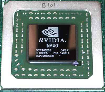
Since we took off the cooler, let's have a closer look at the GPU:
What catches the eye first of all is a huge die: 16 pipelines and 222 million transistors. Another innovation is a frame similar to that used by ATI for protecting their GPU cores from damaging. A die as large as that in NV40 certainly needs such protection.
At this point we finish our description of the card and proceed to the tests.
|
|


