 |
||
|
||
| ||
Revelations from AMD, IBM and VIA about Processors and Other ThingsWe go on with our coverage of VIA Technology Forum VTF 2006, held this summer in Taipei. The Forum offered very interesting presentations and products from the main sponsors – AMD, IBM, Microsoft, Fujitsu, Gigabyte, HP, Kingston, Samsung, and some others.
AMD's Report at VTF 2006Phil Hester, AMD's Vice President and Chief Technical Officer,  reported about its plans on manufacturing processors and promising technologies, AMD designs for its future products (this report was entitled "Driving x86 Innovation Forward"). 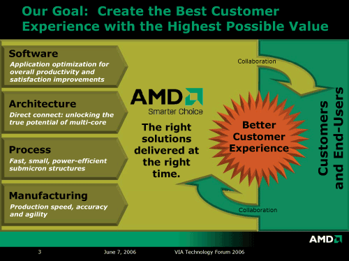 AMD's goal is to create the best customer experience with the highest possible value. For this purpose the company is going to increase its production capacity by up to 4x in next three years. 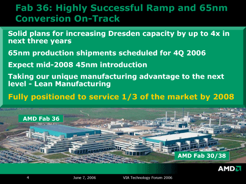 65nm production shipments of SOI processors will start very soon — in the end of 2006 (samples of such processors are already available). AMD and IMB plan on introducing 45nm technology in mid-2008. The company advocates modular design for its platforms: 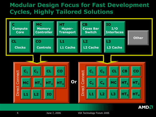 AMD pins its nearest hopes for a technological break-through on quad-core processors to launch in 2007. They will offer the following advantages: 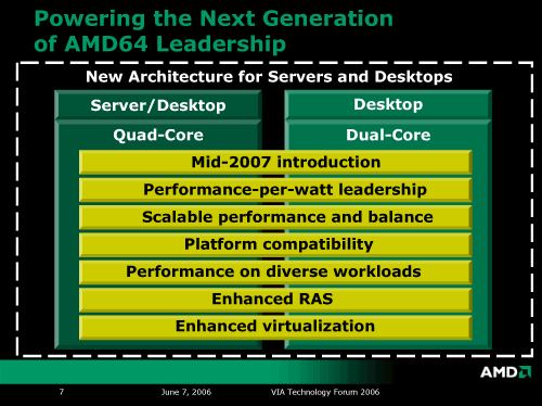 Phil also showed a die of the future quad-core processor from AMD (codenamed Deerhound). 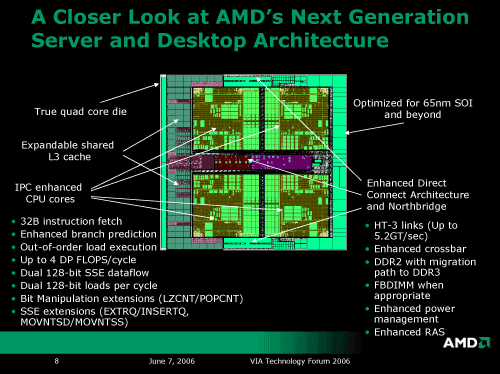 AMD stresses that, unlike Intel, it offers a truly quad-core architecture. It's not two independent dice in a single package (like in future Intel Core 2 Quad), but a single die with four cores and shared architectural units, including shared L3 cache. Dynamic Independent Core Engagement (DICE) technology in these AMD processors allows to dynamically and individually adjust core frequencies for improved power efficiency without deteriorating performance. 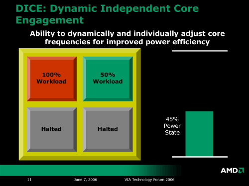 Performance-per-watt progress of AMD processors will go on, reaching +60% in 2007 and +150% in 2008. 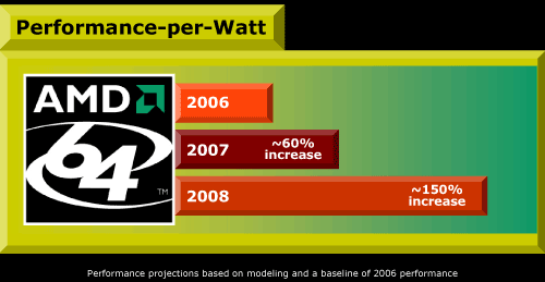 It agrees well with The Green Grid requirements, accepted by many leaders of the IT industry.  Power consumption will be also reduced in the new mobile processors from AMD, which are expected to have a number of interesting innovations. 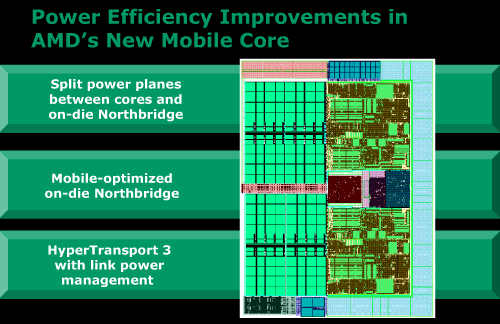 Among such innovations are split power planes between cores (each of the cores can be stopped/started based on application need) and mobile-optimized on-die Northbridge (support for more power efficient DDR2 memory), as well as new HyperTransport 3 with link power management (dynamic throttling based on core states). 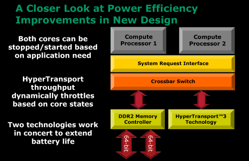 Thus, AMD is about to have architectural and technological improvements for server, desktop, and mobile processors. In future, AMD is also planning to create special-purpose, tuned processors. 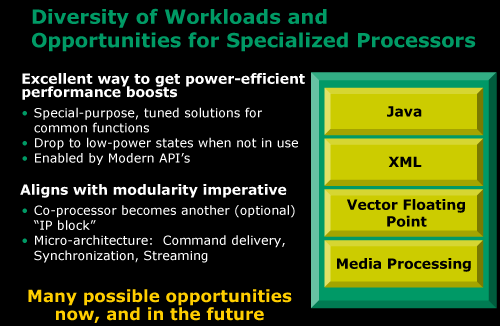 They will allow lower-power hardware solutions due to optimized micro architectures. Such specialized cores may be built into general-purpose processors in future. Mr. Hester also spoke about AMD's plans to design a "4x4" platform for enthusiasts and resource-intensive applications. For example, Direct Connect architecture will be used to create a quad-core multi-socket CPU configuration. Then the company plans on upgrading it to 8-core systems. Another interesting solution - HyperTransport HTX will be used for HTX expansion cards, plugged to a special expansion slot on a motherboard. 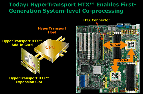 The advantage of this solution over PCI Express or PCI-X buses is that HTX cards will practically "sit" on the high-speed FSB of an AMD processor, that is they will offer higher performance. This solution is currently planned for server systems rather than desktops. But who knows what happens later. ;) I wonder how soon video card manufacturers will decide to use advantages of HyperTransport HTX for designing video accelerators of a new generation? Will ATI be the first and only company here? Another step in the AMD platform development and its compatibility improvement is AMD's strategic initiative named Torrenza, which should give the industry the first x86 customer-centric innovation platform. 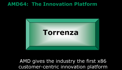 This initiative is based on the open-source principle and involves a lot of notable IT players to create general architectural innovations. Torrenza vision map is published on the picture below. 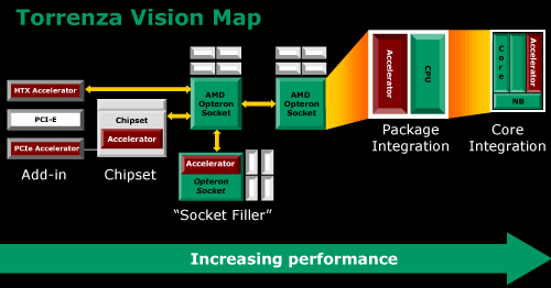 HyperTransport HTX is not the only interesting component here. There is also a specialized accelerator in a socket instead of a usual processor — Socket Filler. There are even third-party designers — for example, DRC Computer and XtremeData announced dynamically configured FPGA chips, compatible with AMD64 Opteron socket (on dual- and multi-processor motherboards), which accelerate specific algorithms of a given user. Along with a calculator, they use static memory and flash memory. The new AMD platform will possess much better options for integrating various units and flexible configuration due to the new solutions. 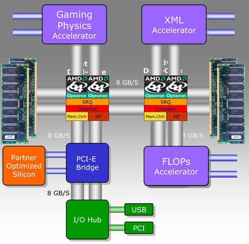 The grand scale of the Torrenza collaboration project is already impressive. We can hope for a break-through in the nearest future. 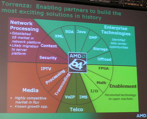 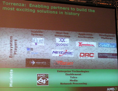 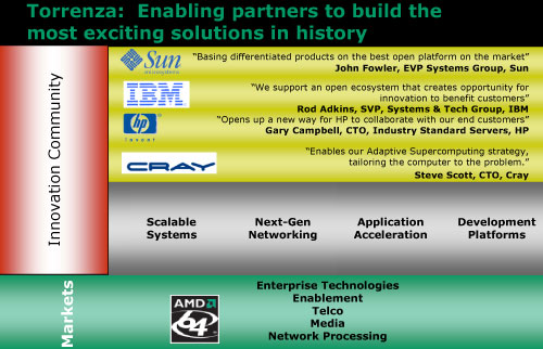 VIA has all chances to become one of the leading players here, especially in the light of the latest event (AMD-ATI merger) - it has rich traditions of chipset building for AMD processors, including professional systems. * * *
Another AMD's keynote address at VTF 2006 was given by Rod Fleck, AMD Fellow, Consumer Multimedia. He spoke about AMD solutions in the field of High Definition Digital Media, which is quickly getting popular in the world. The notion of HD content includes not only audio video and photo materials of such resolution, but also proper games, high-definition video playback / DVR, transcoding / compression of media, multi-room media access, new media client devices. According to AMD employees, the AMD64 dual-core is the ultimate processor for all these tasks, because these processors offer excellent gaming performance, support for multimedia instructions, 64-bit optimization, multi-tasking, and a built-in memory controller. The future MS Windows Vista that also stakes on HD features works well on AMD64 processors. The reporter illustrated his words with benchmarks. 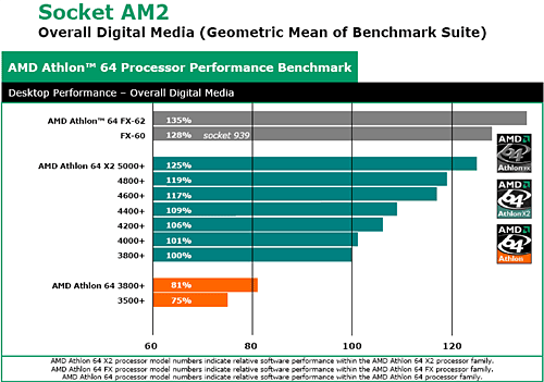 AMD Live! also works in the same direction, it contributes to the appearance of AMD-based personal computers that are fully rigged up to work with this content type.  AMD Live! concept is illustrated by the following slide:  The corporation sees further development of the Live! platform in improving communicative, network, and interactive features. 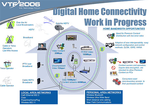 As well as in projecting PC technologies onto traditional consumer electronics, adding HD content and data exchange/translate features, merging several such devices into a single entertainment suite (in a single case). 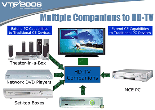   But along with the digital home x86 platform 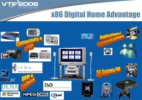 the company should develop various services to fill these platforms with useful content.  The first AMD-based consumer platforms have already seen the light, the product range will expand soon. 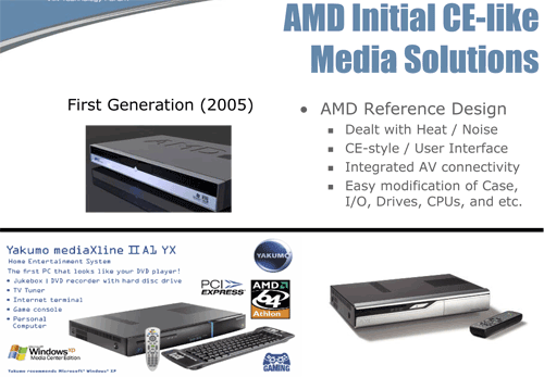 The new AMD Athlon 64 X2 dual-core energy efficient processors can help spread these systems. They can be used in high-performance compact and noiseless solutions. 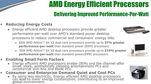
IBM on Semiconductor Technologies for UMPCThe keynote address, given at VTF 2006 by Dr. Gary B. Bronner, Project Leader for IBM's SOI Development Alliance, New York, aroused great interest.  Stanford graduate and the author of over 64 patents, since 2004 he has been responsible for the research and development of IBM's 90nm, 65nm and 45nm SOI technology. These technologies are used by IBM as well as by its partners, like VIA/Centaur and partially AMD. He spoke about the SOI technology that has been used by IBM since 180nm and about its advantages for UltraMobilePC (UMPC) processors, including VIA C7-M processors. SOI 90nm technology (Silicon On Insulator) is currently the main CPU manufacturing technology at IBM. This technology also uses copper wiring with low dielectric constant insulator (low-k). Like Intel, the company uses strained silicon for boosting transistor performance, though the implementation is slightly different. SOI advantages include high performance and lower leakage (less power is dissipated by processors). But it comes at a cost of higher wafer prices. This technology is an excellent choice for UMPC processors. It can be used by IBM's technological partner AMD as well as by fabless VIA Technologies, which is forced to have its processors manufactured at third-party plants. Differences between a SOI transistor and a traditional transistor on a silicon wafer are shown in the picture. 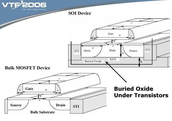 The former is practically separated from the wafer by a thick layer of quality insulator (silicon oxide) to eliminate a number of parasitic effects. There are two methods for the commercial manufacturing of SOI substrates with a working layer (used to create transistors) of high-quality silicon above the insulator: by bonding two substrates together, one of which has an oxide layer (on the left), or implanting silicon with oxygen to form a built-in silicon oxide layer after annealing (on the right). 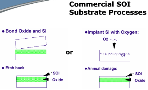 Subsequent creation of transistors on such substrate allows to reduce stray capacitance (oxide below transistor reduces p-n junction capacitance), to shorten transistor gate lengths (better control of threshold voltage), to lower device threshold in order to improve low voltage operation. Besides, such a structure possesses improved isolation, no latchup, and lower leakage at high temperatures. A photo of the real SOI transistor structure is published below. 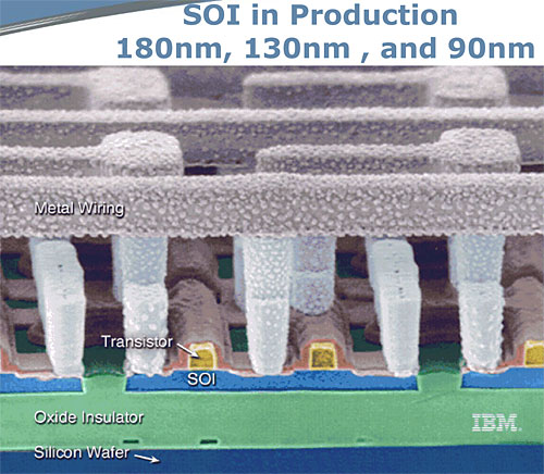 And this is a photo of copper wiring in such IBM dice (colors are added to these photos artificially, to make them readable). 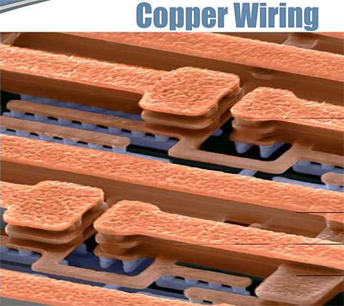 IBM SOI 90nm technology is notable for 46nm channel length, local strain for n-fet 15% performance boost (see the picture), 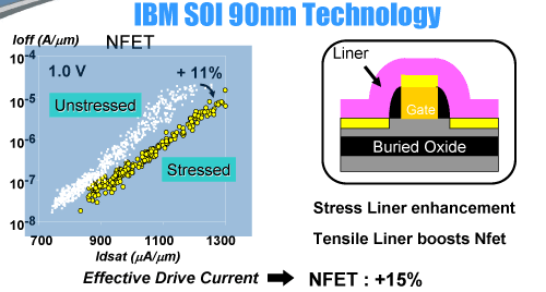 1.0V operation (nominal), dual gate oxide process (11.2A for high performance transistors and 22A for high voltage transistors), local interconnect, 10 levels copper wiring with low dielectric constant insulator - low k (see the details on the photo).  By the way, the similar SOI 90nm process from AMD uses nine interconnect layers. As a result, these SOI structures from IBM are faster by 20-30% than the standard 90nm structures from other manufacturers. This performance advantage can be turned into lower power consumption. For example, 10% performance can be traded for 30% reduction in total power. 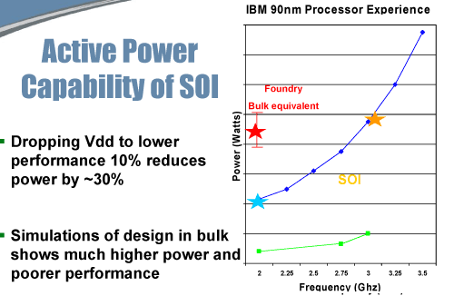 Besides, such transistors demonstrate lower leakages, especially at higher temperatures (see the details below). 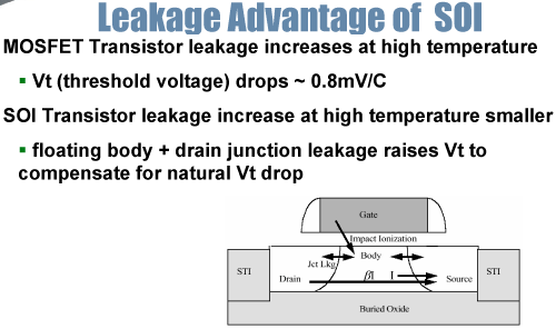 According to the manufacturer, the costs of this process technology are generally lower as well: with a higher substrate cost, SOI dice are superior in processing simplicity, yield of effective chips, cooling costs, and banal power saving. 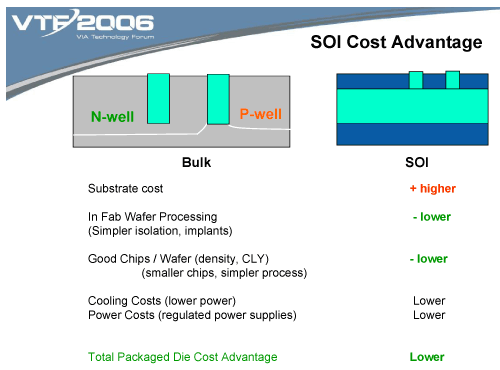 However, as we can see in the recent history of Intel processors, much depends on CPU microarchitecture. It may not be as simple in practice as it seems. Then the reporter from IBM proceeded to how this technology was used to manufacture the latest VIA C7-M processors designed for mobility. Along with the technology itself, the new VIA C7 chips use a number of architectural innovations to reduce the average power consumption. The new features allow to raise the operating frequency of processors to 2 GHz without increasing TDP much. For example, the new processors have the typical TDP level of 20W at 2.0 GHz and just 3.5W at 1.0 GHz under ULV conditions (ultra low voltage). When Windows is idle, power consumption of a processor goes down to 0.25W! Ultra compact package allows to use these processors in the thinnest notebooks and UMPC, though the dice themselves support many modern technologies: SSE3 instructions, 800MHz or 1066MHz FSB, a number of security functions, dual and quad processing. 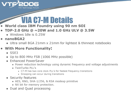 Low leakages in SOI processors at high temperatures are illustrated by the following figures: these chips consume 1.8 times as low power at 50°C as similar dice manufactured without SOI technology (0.3W versus 0.58W); at 100°C this parameter grows to 2.25 times (0.68W SOI versus 1.53W). 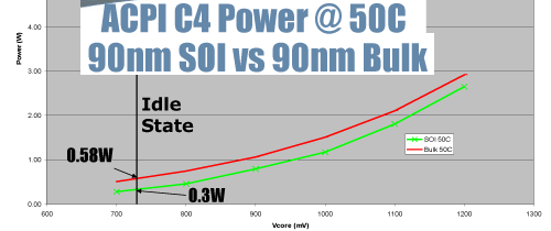 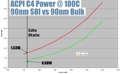 Such high characteristics of the new VIA C7-M products, manufactured by the modern IBM SOI 90nm technology, make them excellent processors for UMPCs. 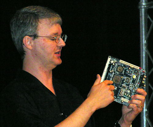 UMPC reference motherboard for VIA C7-M.
We'll talk about it in the next part of our VTF 2006 Coverage.
To be continued.
Write a comment below. No registration needed!
|
Platform · Video · Multimedia · Mobile · Other || About us & Privacy policy · Twitter · Facebook Copyright © Byrds Research & Publishing, Ltd., 1997–2011. All rights reserved. |