 |
||
|
||
| ||
Spring has come... It has brought Intel Developer Forum (IDF) that is held twice a year in sunny California and that regularly visits other cities of the world (since recently – in Russia as well). I've not mentioned spring for effect only – it's really warm in San Francisco, where IDF is held from the 1st to the 3rd of March in a huge conference center Moscone West. 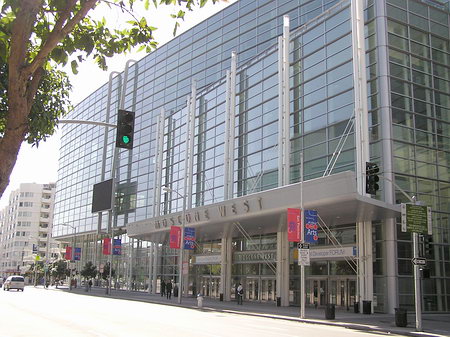 Trees and bushes are in blossom exhaling spring fragrance and citizens of this city wear shirts or jackets outdoors, if it doesn't rain. Having arrived at this lovely scenery from snowy Moscow, it was rather difficult to sit up all days in conference halls and press rooms, to lounge about thousands of visitors and IDF organizers in the lobby and show cases. If not for the unique and grasping information, which simply pours on you, leaving you not a single minute of rest. Even me, the regular attendee of central Intel Forums (as well as many other exhibitions and conferences on the similar subjects), who seems to be fed up with such events and who takes them almost like another Hollywood block buster, made up of long-known cliches, is often surprised at the flow of innovations prepared by organizers for IDF participants. Surprised and sometimes even delighted...  Our constant readers probably don't need to be explained what Intel Developer Forum is. It's an activity regularly conducted by Intel and its closest IT allies for many years already. It's notable for some peculiarities that differ it from various computer expositions (like CeBIT, Computex, Comdex or CES, where hundreds and thousands of IT manufacturers boast of their achievements for marketing purposes) as well as from large world scientific and technical conferences (like Material Research Society Meeting, IEEE and others, where hundreds of the leading world-level institutes and research labs announce the latest scientific discoveries, inventions, and technologies, which will take still many years to apply in industry). In my opinion, IDF is actually closer to the latter rather than to the former. That's because Intel, annually spending over 4 billion dollars on Research & Development, does not try to demonstrate at IDF its current products, ready for manufacturing (microprocessors, platforms, and so forth),  but rather tries to inform the industry about the vector it will take to develop in the nearest years. To promulgate the current and future technologies, which the corporation applies together with its partners and other IT developers, to win new researches and engineers (that is "developers" – judging from the Forum title), and probably to discuss expedience of some steps within the entire IT community. And though IDF still shares some of the "exhibiting-marketing" character, its research and technology part is the most valuable and interesting to my mind. So Day Zero of the current IDF on February 28 brought several surprises for the leading press and analysts all over the world. I shall try to write about them in this coverage, which forestalls the account of the Forum itself. Silicon nanotechnology: looking into the next 20 yearsThe first report on Day Zero dealt with possible ways of development of silicon technology for manufacturing computers in the nearest decades. In a few primitive words it can be called "extending Moore's Law for the next 20 years", but this seemingly trivial issue has been supported by breath-taking details about nanotechnology research and its industry applications. This report was presented by Paulo Gargini (see the photo), the Director of Intel Technology Strategy and Intel Nanotechnology Research.  This presentation took over an hour and was conducted in a very quick tempo. There was no time to collect oneself and speculate over a slide. Its detailed account would have been useful for some of our thoughtful readers. But it would have been very long (it's about a hundred of "solid" slides, each of them needing a lot of comments). That's why I will only note the most interesting (to my mind) points, especially as some of the details have been already described in the articles of my colleagues and my articles about the previous IDF and recent "technological breakthroughs" from Intel. Maybe I will provide more details next time. For the last 40 years the number of elements on silicon dies has been steadily doubling each two years and the cost of one transistor on a die has been going down at the same pace.  About ten years ago scientists foretold big problems for switching to 100 nm devices, but fortunately none of it happened. These days industry leaders possess well-explored prospects of traditional silicon technology development with planar CMOS-transistors for 10 years onward (see the slide). 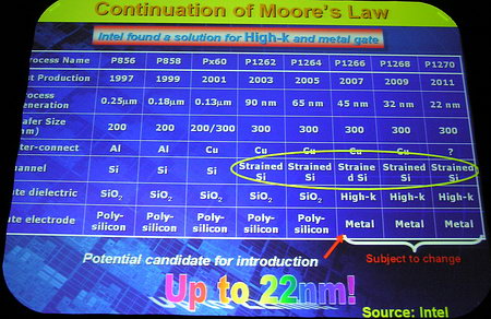 The need for principally new electronic devices will arise only by 2013, when CMOS device scaling capacity is depleted. 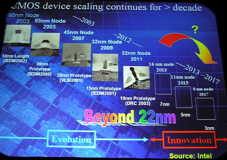 The new silicon devices include multi-gate (for example, tri-gate) nano transistors, devices on silicon nanowires, completely surrounded by the gate, as well as devices with quasi-ballistic transport.  In the longer view there might appear c-nanotubes, just several nanometers in diameter, which may serve as metal or semiconductors depending on their structure. What concerns nanoelectronics, there are interesting devices based on InSb heterostructures (with uniquely high mobility), see the slide. 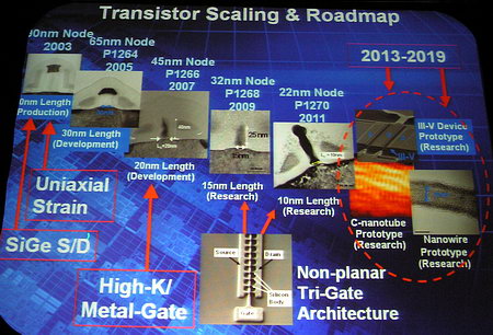 And what will happen after 2020, when the CMOS technology depletes its scaling potential, having reached the atomic limit? 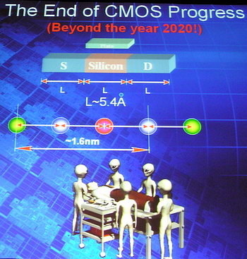 In this case it will probably be spintronics – operating magnetic moments of elementary particles:  There is a talk of quantum computers. But the CMOS technology is still alive and Moore's Law will continue at least for the next 15-20 years. 
Silicon photonics: a new breakthroughA report about the first in the world continuous all-silicon laser created by Intel has become another interesting IDF event of Day Zero. Strictly speaking, this piece of news spread all over the world a couple of days before IDF (a paper in Nature and Intel press release were published February 17), but here the key designers of the new device shared with the audience many details, unknown up to now, and demonstrated multiple dies with such lasers. For example, a die on this photo (taken by the author) contains eight such lasers. 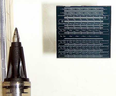 I'll note without going into details that in order to create such a silicon laser, Intel scientists had to solve an important problem – so called "Two Photon Absorption", which previously hampered the creation of a continuous all-silicon laser.  The use of silicon as a material for creating a laser and for multiple amplification of IR-emission (due to a huge Raman effect, about 20000 times),  was previously problematic, because Raman gain entered saturation at powerful pumping and the obtained saturated capacity was not enough to create a continuous laser. 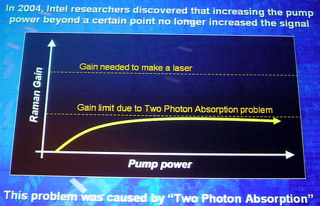 The fact is that the energy of one infrared photon (light quantum) is not enough to knock out (to free) an electron at a collision with an atom in a silicon lattice. But if two photons collide with an atom (which often happens when a laser is pumped with external emission), atom ionization becomes possible and free electrons in silicon start absorbing photons on their own, thus preventing further Raman gain. They managed to solve the problem by incorporating a so called p-i-n structure along the optical channel (silicon area with hole and electronic conduction correspondingly at the sides of the undoped optical channel in silicon, see the picture). 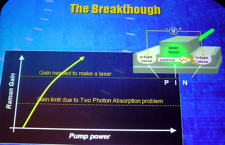 Applying electric displacement between p- and n- zones in silicon, "two photon" free electrons can be effectively removed from the optical channel area, which considerably increases Raman gain in silicon and creates a continuous laser. This solution can be used to create two important optical devices right on a single silicon die – an amplifier and a modulator.  Cascaded mirrors (placed right on silicon) also allow to create multiwave optical communications channels and compact lasers for a variety of applications.   Mario Paniccia, the Director of Intel Photonic Technology Lab, holds a die of the new continuous all-silicon laser (on the right) and a traditional expensive Raman optical amplifier (on the left):  This Intel achievement opens up new horizons for silicon photonics development and its integration into the traditional microelectronics. 
Write a comment below. No registration needed!
|
Platform · Video · Multimedia · Mobile · Other || About us & Privacy policy · Twitter · Facebook Copyright © Byrds Research & Publishing, Ltd., 1997–2011. All rights reserved. |