|
||
|
||
| ||
|
||
|
||
| ||
 What makes this article special is that is has no introduction or conclusion. Perhaps, it symbolises a continuity of technical progress in this sphere. Or, perhaps, it doesn't symbolise anything. Three commandmentsThere are three factors that have the primary influence on the architecture of modern hardware graphic solutions:
Although these sentences may sound trite, I suggest you meditate on them as it is there that the understanding of modern graphic architectures and their development is hidden. Meditation on themMost primary data modern computer graphics deals with (vertices, vectors, colour values) are vectors. Interestingly, their dimension almost never exceeds 4. And it is no less interesting that statistically, most operations executed by an accelerator are usually vector ones, 3D or 4D. That is why modern accelerators almost exclusively consist of 4D vector ALUs that execute one operation on four components of this or that format. To illustrate it:
We need to add two colours. Each of them is a 4-component vector: R, G, B, A — red, green, blue, and optional alpha coefficients of transparency degree.
Obviously, because the data do not depend on each other during these calculations, we can execute them in parallel, that is, in one step. And we don't need four normal ALU to do it, we can use just one vector ALU (the so-called SIMD: one instruction, many data) that would have common control logic and could execute one operation on four source data sets. But it's all much more complicated in reality. First, the data may begin to interact. For example, we want:
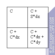
to estimate the red light of the result as a sum of the green and the red component of the source data. For this, we need to use the ALU to realise random commutation of vector components before they are processed:
Thus, we save the time of data transfers. And although we can make a separate operation to rearrange the vector components instead of making the ALU so functional, our approach is more rational in terms of performance.
But let us not stop our meditation here, as it's just the beginning. In real graphic algorithms, we may be discontented with the fact that all the components are subjected to one and the same operation. For example, the A component is often processed by different rules:
Here we must make up our mind. We can either divide this operation into two successive ones or to make our ALU execute 3+1 (RGB+A) operations, which is, in fact, equal to having two ALUs: a three-component and a two-component ones. Of course, it is more complex but it often brings about a performance gain as two operations are executed practically in parallel, within one.
The next step is to let these operations be executed on random components and depend on neither 3+1, nor 2+2 schemes:
In real tasks, we'll come across the situations where we'll have to process only 2D vectors or scalar values (especially in the chip's pixel pipelines and pixel algorithms), and then we'll be able to optimise our calculations and execute two operations simultaneously. And it will be nice if even in this case half of ALU transistors aren't idle but are busy with some other operations. Thus, modern graphic ALUs are up-to-4-component vectors that enable a random rearrangement of their components before calculations and can execute different operations on 3+1 and 2+2 schemes. But component parallelism is just the first level: we are limited by 4 components. Whereas the most attractive thing about graphic algorithms is that objects processed in the graphic pipeline are usually independent of each other. Let's take, for example, triangle vertices. All three vertices will be processed basing on one algorithm and the order of processing is of no importance (when operations are being executed on the second vertex, we're never interested in the results or the course of the first processing). Therefore, there are no obstacles for us to process several vertices simultaneously. That is why modern graphic accelerators can have 3 or 4 vertex processors. The picture with pixels is even more optimistic: as we know, there are many more pixels to fill than vertices to transform. So, modern accelerators can process 4 to 8 pixels simultaneously, and future ones will surely process more than that.
There is one important thing here. If the processing algorithm provides for no check of conditions during the execution and the operations on all vertices or pixels are always the same, then it's all simple as that:
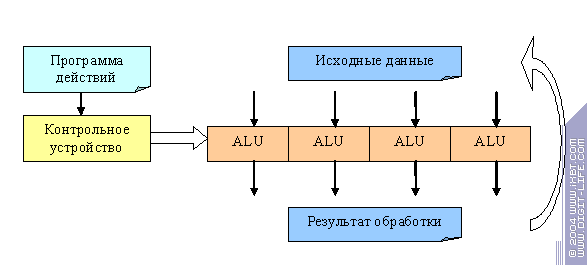 We have a control device that acts according to a certain instruction and prepares the ALU set for some operations and several objects (e.g., pixels or vertices) processed in parallel. The device configurates the ALU to execute an instruction and all the data go through it in parallel, step by step. Then the device configures another instruction and so on, until the program is exhausted. Such programs can be very long in modern accelerators, they are called pixel/vertex shaders (depending on the objects they deal with). What is nice about all this is that there can be any amount of data and any number of ALUs (within sensible limits), which enables us to increase the power of the accelerator by simply cloning the ALUs. And we still have one control device which allows us to use less transistors. However, new standard DirectX shaders (pixel and vertex shaders 3.0) have certain conditions. Processing can be different depending not only on the constants (which is, in fact, nothing but an illusion of choice, as all vertices and pixels are processed identically) but also on the source data we have. It means that we can no longer use one control device for all ALUs. Thus, we need to create really parallel processors that would be guided by a common instruction but would execute it asynchronously. And it's here that troubles appear, such as, for example, synchronisation issues. Some vertices or pixels can be processed within a fewer number of operations than others. So, what is better: to wait until all objects are processed or to start processing new objects as the processors are getting free? The latter approach provides for a more optimal use of hardware but requires a more complex control logic and consequently, more transistors.
However, a compromise is also possible here. We still have one control device and each object passes through the same set of operations. But if a certain condition was fulfilled or not, the results are either accepted or removed without changing the state of the object. Thus, we execute all possible condition branches (both "yes's" and "no's") with half of our actions being idle. But we don't lose synchronisation as all the objects are processed simultaneously, being controlled by one device:
The convenience of such approach depends on the share of conditional operations. In our case, 6 operations out of 20 were idle. Soon, as graphic data processing programs become more flexible, the profit will diminish and finally, fully independent processors will be the most preferrable. But for the time being, the compromise seems quite to the point. The deeper we get into the meditation the more we understand that even object-level parallelism is not the last step to performance increase. We can introduce a rather paradoxical notion of time parallelism and show that trading bad for worse can sometimes bring considerable profit. This is a typical succession of actions during pixel filling:
Texture selection (and also filtering, texture coordinate preparation, MIP level estimation and other actions) can take over a hundred steps and last more than a hundred clocks. Of course, we can't be contented with this state of affairs, but it is due to the independence of pixels that are processed in parallel and will be processed later that we can create a more-than-a-hundred-stage-long pipeline which would only deal with texture selection and provide a result per clock if everything is all right. In CPUs, ~20 stages is considered a lot and data processing itself takes not more than 2..3 stages. But the independence of pixels enables an effective use of such long pipelines in graphics, hiding huge latencies of such operations as texture selection. And this is what can be called "time parallelism" :-) However, modern graphic algorithms become increasingly flexible. Now we have the notion of a dependent texture selection, where selection coordinates are specified separately for each pixel — probably, right in the pixel processor, basing on previous selections:
Even a very long pipeline won't save us in this situation. Having started to select the second texture value, we can't execute the shader till the selection is completed. So we'll have to wait about a hundred clocks during which we won't even be able to start the second part of the calculations ("More calculations") as they are probably dealing with a value selected from the second texture. So, what do we do? Let us get back to time parallelism. We can create a more-than-a-hundred-pixel-long queue of objects prepared for processing beforehand. Then we can take one shader instruction, run ALL our pixels through it, and store the resulting data (for this, we'll need a large pool where intermediate data for the whole queue will be stored). Then we'll take a second instruction and run all our pixels through it and so on, until the shader is completed. Thus, we'll have a situation where an instruction can be executed in a hundred clocks but it will be supplied with a very long pipeline that will give out a result per clock, irrespective of whether other shader instructions are waiting for the previous results or not. This means that texture selection latency, as well as latency of any other operation will cease to exist for us, as we can deal with over a hundred pixels within one instruction (operation) before the next one.
This is the scheme we have:
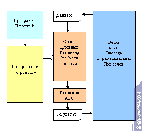 We'll come back to it later. What is paramount for us now is that independence of pixels/vertices enables us to exploit different variants of parallel processing, making graphic accelerators more effective. To the extent that they can give out multiple new results per each clock even in the case of relatively complex procedures.
The last point we'll dwell upon during our meditation concerns provision of the source data. It is a truly burning issue for GPUs. As we know, memory technologies do not develop as swiftly as computative power, and there is only one pleasant fact (a streaming character of graphic algorithms) that enables us to provide modern accelerators with data. A GPU is like a funnel: a lot of various data at the entrance and one resulting image at the exit. All the incoming data are streaming, they are read serially or almost serially in a more or less convenient way. Consequently, they can be cached, preselected, queued, etc., not to let the memory subsystem be idle and to increase its efficiency. Luckily, modern accelerators have virtually no random access to the memory as it "kills" caching effectiveness. Thus, in contrast to CPUs, GPU caches are relatively small, separate, and mostly read-only. This makes them increasingly effective: even a frame buffer cache can be divided into two parts, one of which will be read-only, and the other one will be an ordinary write queue. 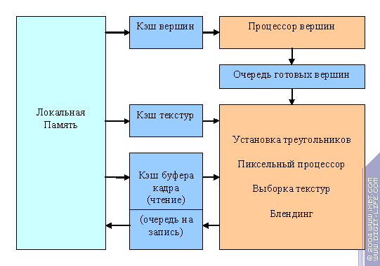 And this is where our meditation smoothly merges with reality. Reality and our conceptions of it Using modern DX9's of NV3X and R3XX families as illustrations, we'll see how our meditation priciples are (or can be) brought into life. Many architecture details mentioned in this article are nothing but our guesses as accelerator developers are not too willing to share them with anybody. So, read this at your own risk: we don't guarantee anything.
First of all, to understand HOW it all works, let's look at the logic structure of the accelerator (a graphic pipeline):
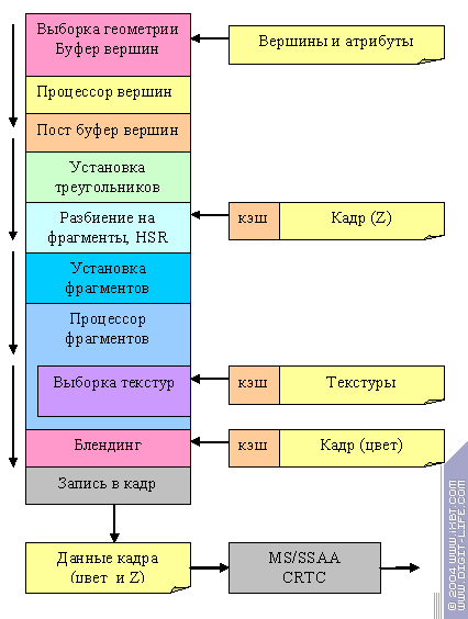 The way the image is being built:
Now it's time we dwelt on vertex and pixel processors. But before that, let's discuss some peculiarities of practical realisation.
This is a schematic of a modern accelerator:
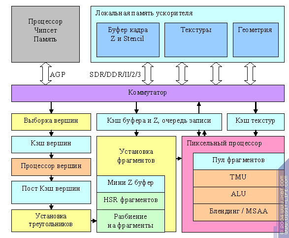 It is the multi-channel memory controller that catches the eye first of all. Instead of one very long 128/256-bit memory bus, it uses two or four fully independent ones with a 32 and 64 bit width, respectively. What was it done for? Let's take a closer look at the data flows that pass while the accelerator is working. As a rule, textures and geometry are only being read, the frame buffer (colour) is only being written, and the Z buffer is being both read and written. So we have 4 continuous data flows. If we manage to place them (partially, at least) in different controllers, we'll get a substantial gain in terms of latency time at data access. We won't have to switch the memory back and forth (from read to write modes) and "go bufferhopping". And that, in turn, means that we can make very small and effective caches. Their typical sizes (presumable or found experimentally) would be as follows:
And that is an important difference between GPUs and CPUs. The streaming and predictable character of the data enables us to do with small but very effective caches. The data (frame buffer, Z buffer, textures) are often stored and selected in rectangular blocks, which makes memory operations more effective. Most transistors are spent on multiple ALUs and long pipelines, which puts considerable restraints on clock frequencies: a synchronous work of a specialised complex pipeline over 100 stages long requires substantial deviations from an even signal spread. That is why several-GHz frequencies typical for CPUs are yet unachievable for GPUs.
Vertex processor
It is a sort of summary of our knowledge about modern vertex processors:
Comments on the table:
In general, it is obvious that while an R3XX vertex processor realises stanbard 2.0 almost "to a T", an NV3X one all but reaches vertex shaders 3.0. We'll dwell on shaders 3.0 in our DX Next article; as for the current one, we'll only mention that the main difference which somehow wasn't realised hardwarily (or included in 3.0 specs) is the possibility to access textures from the vertex shader. Other differences in realisation include such subtle things as hardware support of SINCOS or EXP calculations (replaced with macros of several instructions in the base DX9), but we won't go that much into details. The main difference remains dynamic control of shader execution in NV3X.
Evidently, to realise an R3XX vertex processor, we can choose a scheme with common control logic but several parallel ALUs that process several vertices simultaneously, basing on the same instruction. There are no dynamic jumps and no predicates, the constants aren't changeable and can be used together. This is what a vertex processor of senior R3XX models looks like:
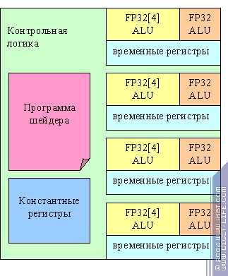 Apart from common control logic and separated constants, we'll also note two ALUs: a 4D vector one and a scalar one. They can work in parallel, executing up to two different mathematical operations per clock. This strange configuration (5 ALUs on a 4+1 scheme instead of 4 ALUs on a 3+1 scheme) was probably predetermined by the need to execute a scalar product quickly and then generalised to a full-value superscalar execution. Junior RV3XX chips have two sets of ALUs and registers instead of four.
In principle, NV3X must contain separate, independent vertex processors, at least the presence of dynamic execution control is a good reason to suggest it. However, there are a lot of things that indicate a quite another picture. An NV3X vertex processor is close to what we've seen in the latest 3dlabs chip. Let's try to draw its presumable scheme:
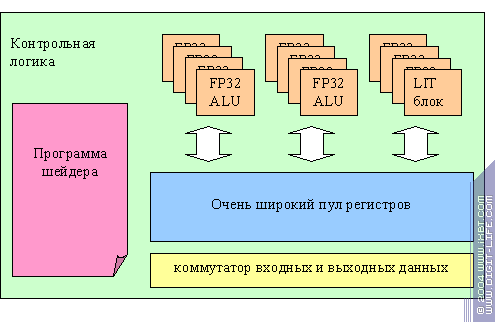
Now we'll voice our presumptions. Actually, we have a very wide array of independent scalar floating-point ALUs, a very wide register pool, and a shader instruction written as a VLIW microcode that specifies actions for each next clock for all ALUs. What are the merits and demerits of this approach? On one hand, we can make an optimal distribution of computation resources, processing several vertices, including a maximal use of all ALUs by means of different tricks with the microcode compilation where different operations for different vertices are executed simultaneously. If the shader is less complex, we can process more vertices simultaneously as more registers become free. It's easier for us to include specialised units (e.g. in order to accelerate a fixed T&L) into this scheme. On the other hand, what to do with flexibility? We can't manage all these devices separately, in several flows, depending on dynamic conditions. There are two ways out here: first, we can build all dynamic conditions on the predicates, supplying each line of the VLIW microcode with a set of 4 or even more predicates and creating corresponding registers. Second, we can go farther and realise several (e.g. 2) instruction counters (flows) in the control device. But in most shaders that have no jumps or dynamic control of execution, we can use just one instruction flow although with the maximal efficiency and on the maximal number of vertices. We don't know the truth, but at least, we shared our ideas with you. Vertex processors in junior
NV3X chips can be scaled in a very subtle way: starting to narrow down the register pool and reduce the number of ALUs and functional units.
NVIDIA officials say that NV31 and NV34 vertex processors show a 2.5-time slower performance than senior models. The NV36 vertex processor has been taken from NV35 and underwent no changes; its performance allows no compromises. What was it done for? Obviously, its performance is superfluous for a game mainstream card. But don't forget that the same chips serve as a basis for professional NVIDIA and Quadro FX solutions where vertex performance is often crucial. On the other hand, in contrast to the fragment processor, the vertex one uses fewer transistors, and the most effective variant can be installed in a middle-price solution. Pixel (fragment) processor
We'll start with a table once again:
So, NV3X look much like a leader in terms of specification and flexibility. But we know too well that in practice, it's all the other way round in terms of performance in pixel shaders 2.0. Complexity comes at the expense of a long debugging and optimisation of the compiler in the drivers (the latest visible increase in shader speed was some months ago) and peak performance as well.
And now we'll show you the most interesting thing. This is a schematic of an NV35 fragment processor pipeline (we aren't giving you many details as they add nothing to the description of the process):
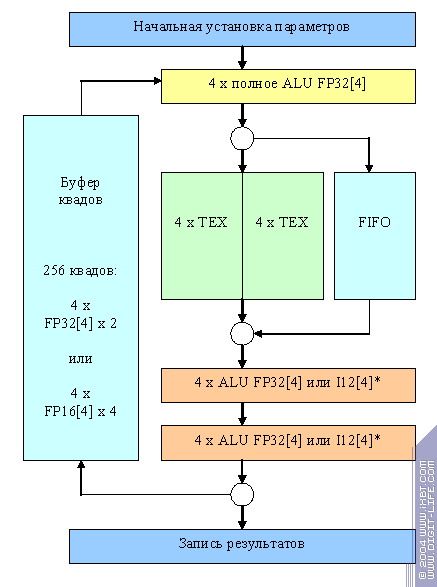
How does it all work? Several hundred 2x2 quads are being processing simultaneously. As far as the fragment processor is concerned, a quad is a structure of data, that contains the following information for each of four pixels:
All the quads pass one by one through this long pipeline consisting of an ALU, two texture modules and two more ALUs. The length of the pipeline is over 200 clocks most of which (~170) is needed for texture selection and filtering and is hidden in the texture units. The pipeline is capable of delivering one quad per clock in a normal mode. So, one turn of this giant round can execute (or not execute) the following operations for each of the four quad pixels:
Then, if two texture selections and three operations aren't enough, the quad can go round through the quad buffer to reenter the pipeline. In modes compatible with older applications (FPP and shaders up to 1.3), integer capabilities of the mini ALUs are used while the floating-point ALU helps to calculate and interpolate texture coordinates. In this case, two temporary registers per pixel are always enough (specification limits). Now let's examine how shaders 2.0 (and 1.4) are executed.
Pixel shader microcode instructions are selected one by one from the local memory of the card. One nicrocode line configures the whole pipeline, including two texture selection and filtering modules and three ALUs set identically for each of the four quad pixels. Then all the quads go through the pipeline. After this, the pipeline is configured to a new set of operations and the whole thing repeats. Thus, the shader compiler has a lot of work cut out for it: it must try to gather shader instructions into packs that would use pipeline resources as fully as possible. This is the shader's code:
It will be grouped into two microcode lines (the brackets contain the number of the source shader line):
The effectiveness is amazing: a nine-line shader was grouped in just two clocks. But there is some pitfalls here as well:
The last point needs to be explained. The thing is that temporary registers are used during calculations. Formally, there are 32 of them but in reality, only 2..4 temporary registers are normally used for this or that operation. And that makes a great difference for NV3X. If we want to combine our instructions into one microcode line and ensure their execution within one clock, we have to see to it that all of them should use not more than two FP32[4] (or four FP16[4]) temporary variables in total. And this is what makes performances of FP16 and NV3X-based FP32 so different. It's not about the ALUs, it's all about the number of available temporary variables. If we exceed this limit, we'll have to make another round turn, dividing the pack of instructions into two (which takes one more clock). Or else, we'll have to use two quad structures to represent a real one, which will again double the number of clocks. That is why NV3X is so sensitive to manual optimisations of the shader code and to the quality of the built-in compiler. We can write effective shaders only if we have a perfect understanding of fragment processor architecture. ATI R3XX has a much simpler architecture (see further) and it only takes a standard set of rules to write an effective shader. But then again, it can execute fewer operations per clock.
Interestingly, the above scheme of the NV35 (and, consequently, NV38) fragment processor was a sort of a correction of past mistakes. This was the supposed scheme of NV30:
 There were only integer mini ALUs! Although they were more productive, as
floating-point arithmetics requires more pipeline steps and integer mini ALUs benefited from using the then free steps. They could execute a MAD operation (addition and multiplication simultaneously). On one hand, it sometimes allowed to show higher results in FFP and PS1.1. On the other hand, results in PS2.0 were neraly always lower. Evidently, NV3X developers mostly focused on performance in DX8 applications, thinking (not without grounds) that PS 2.0 will spread slowly in real applications (not tests). But negative response form analysts and enthusiasts largely caused by low performance of shaders 2.0 was an impetus to "correct the mistakes", so to speak, and replace integer ALUs with floating-point ones. Now let's speak about shortened chip versions. This is, presumably, what NV31
looks like: 
In most cases, the chip works as 2x2, i.e. operates with so-called "half-quads", at least when they are passing through the pipeline that has twice as few ALUs and texture units. However, there is a special 4x1 commutation mode that can be available only if there is no round:
 It is fit for simple one-texture filling tasks that demand much fillrate and few intellect from the pixel processor. In fact, this is the main class of tasks where the 4x1 configuration looks better than 2x2. So, NV36 differs from NV31 by mini ALUs, as was the case with NV35/38.
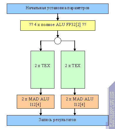
Now we'll show you a presumable scheme of an R3XX pixel processor. In fact, the chip has two separate quad processors. They work asynchronousally and moreover, one of them can be switched off (shortened chip versions known as 9500 were the result of blocking one working or not working quad processor). Well, this is one of the two R3XX processors:

The main difference is that the fragment processor really looks like a processor, not like a big loop, which was the case with. It executes shader operations (up to three operations per clock on four pixels: two arithmetic ones (3+1) and a texture value request). But if arithmetic operations are executed quickly, we can't wait over a hundred clocks of texture selection and filtering. Therefore, the number of quads simultaneously processed is big here too, though it's not so evident. The shader is divided into four independent phases (with the microcodes stored right in the pixel processor, which causes the restraint on dependent texture selection depth), and each phase is executed separately. During the execution, there is a growing number of requests to the texture processor. Thus, a certain number of simultaneously processed quads (though they are processed consecutively from the pixel processor's point of view) makes up to four accesses to the texture processor with a task packet. To all appearance, this number is considerably lower that the one we saw in NV and as a result, the queue is much shorter too. The expense is a potential latency during dependent texture selections. The profits are a much simpler pipeline scheme, a possibility to make more pipelines, and the absence serious problems with the temporary registers. It can be debated what is better. Some will choose a good performance on almost any shader (ATI) complying with the general DX9 principles. Others will prefer a higher performance on a shader (NV) specially optimised for concrete hardware, although they run the risk of getting a times lower performance on a bad code (in terms of the compiler). In total, considering eight R3XX pixel pipelines, ATI won this stage of the battle, at least in what concerns pixel shaders 2.0, which is proved by the test results. As for 1.4 and certainly 1.X, NV3X looks much better here.
Obviously, future generations (NV4X and R4XX) will consider the lessons of the present. First of all, the following problems are likely to be solved: a low number of temporary registers in NV and a low number of ALUs in ATI.
Alexander Medvedev (unclesam@ixbt.com)
01.06.2004
Write a comment below. No registration needed!
|
Platform · Video · Multimedia · Mobile · Other || About us & Privacy policy · Twitter · Facebook Copyright © Byrds Research & Publishing, Ltd., 1997–2011. All rights reserved. |