 |
||
|
||
| ||
Recalling the former GPU manufacture leaders and summarizing the year we can state that Matrox is no more among serious 3D graphics suppliers. All this previously glorious company could release was Millennium P750 and P650 in April based on Parhelia 512 "halved" down to the level of Parhelia LX and Parhelia HR256 in September. 
The main difference between these cards is that P750 supports TripleHead output similar to Parhelia 512, while P650 supports only DualHead familiar from G400. Besides the paired down pixel pipelines, 256-bit GPUs have 128-bit memory buses and are shipped with 64MB DDR. The HR256 model has 256MB of 256-bit DDR SDRAM, 33/66MHz PCI bus, supports resolutions up to 3840x2400. Model's essential is two LFH-60 connectors for up to 4 monitors.  As it turned out closer to the year-end, none of Parhelias obtained DirectX 9 support. What's the saddest this wasn't even planned for the future frozen on DirectX 8.1 and OpenGL 1.3. Therefore at the moment we can exclude Matrox from the list of modern graphics suppliers. Another outsider was S3 Graphics, which from the Autumn of 2002 to the end of 2003 was working on its DeltaChrome DX9 GPU. The latest promises sounded at Computex 2003 already mentioned DeltaChrome's PCI Express support. Manufacturers obtained working DeltaChrome chips in more or less volume quantities only in the late 2003. The "junior" period of S3 Graphics' DeltaChrome finished only in January 2004, when we saw the first solutions on S3 DeltaChrome S8 GPU. 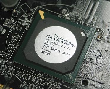
In general the DeltaChrome series includes at least two GPU versions, with 8 and 4 pipelines, 1 texture module per pipeline. Initially the company established the production of 8-pipeline S3 DeltaChrome S8 for middle-end cards and scheduled volumes of the more powerful S8 Nitro to some later moment. 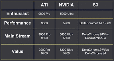
Mainstream 4-pipeline solutions are to be named DeltaChrome S4 and S4 Nitro, while the high-end 8-pipeline models will be named DeltaChrome F1 and F1 Pole. High-end GPU clock speeds should start from about 315MHz, while the mainstream - from 275MHz. As for the memory interface, it should be 128-bit, however 64-bit variants are also possible. According to the features promised for one of the first DeltaChrome S8 novelties, fanless SS8-D3L from C.P. Technology, the GPU works with 256MB of 128-bit DDR and has 300/250 MHz (500MHz DDR) clock speeds. The novelty bases on a 6-layer PCB, has D-Sub, DVI and TV output, and supports resolutions up to 2048x1536. I think prices for such cards (even with 256MB) will initially be about $150-160. 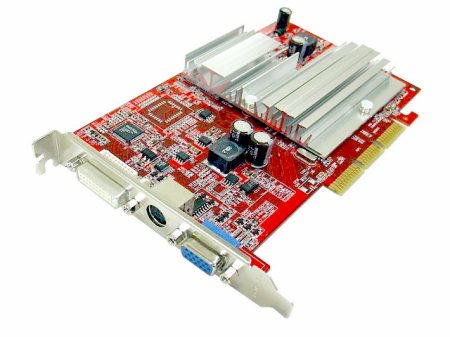
The prospects of DeltaChrome series is still cloudy: S3 Graphics spent too much time outside the desktop performance market. It's hard to make forecasts without knowing company's existing potential. However, the first step into the current 3D market is better than a complete refusal demonstrated by Matrox. What a difference was the Taiwanese XGI Technology (eXtreme Graphics Innovation). The history of this company is still veiled in obscurity: like the 99.9% of shares are owned by SiS that completely curtailed its Xabre II graphics project; somehow there was some money to finance graphics development; somehow there's even enough funds to order volume production of these GPUs. Still I hardly believe in the start from nothing, especially looking at S3 Graphics that didn't even have to start like this. Where from did they get so many talented and creative engineers and how much man-hours it really took to develop a whole DX9 GPU family. This we still don't know. Maybe if XGI succeeds (or fails?), it will share its secrets with us. And at the moment the young company makes all efforts to achieve enough recognition of its brand and looks for graphics card production partners. 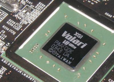
XGI is really ambitious: according to its president, already in 2004 the company is to take over 5-10% of the market. From the angle of buyer, I'm only happy about the new player and stronger competition that will surely press down the prices. But from the point of company's actual finance, it's hard to shake off the sound scepticism. Even with excellent chips and theoretically possible good promotion, it's hard to believe that a company can in a year rush into the market and bite off a noticeable share of this multi-billion market. Well, once all of them companies were starters... 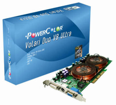 For the sake of justice, I'll mark that we'll be able to call XGI a debutant only in 2004, as the first Volari Duo V8 Ultra shipments launched in December 2003 were only a claim for the future, not the serious market presence. Besides, the maximum GPU/memory clock speeds of 375/500MHz were good only for 2003 solutions, not for 2004 ones.
Company's future plans include the release of mainstream XG42 DirectX 9 core to replace Volari V3 and V5 in H1 2004. In their turn, Volari V5 Ultra and V8 are to be replaced by XG41 core. The most powerful V8 Ultra and Volari V5 Duo Ultra should be replaced by XG45 and XG46 optimized for DirectX 9.1 in about H2 2004. Finally, early in 2005 we should see the XG5X graphics core supporting DirectX 10 that will replace Volari Duo V8 Ultra. 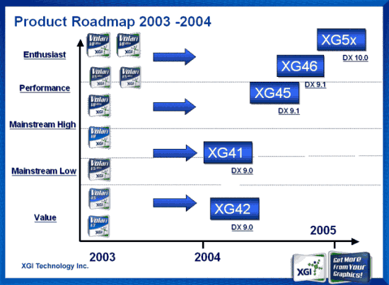 Looking at the GPU series changes of 2003, I ask myself how significant graphics card performance changed and how far the top models advanced. Speaking of ATI Technologies, I remember that desktop Radeon 9800/Radeon 9800 PRO, Radeon 9600/Radeon 9600 PRO, and Radeon 9200 GPU announced in March were the leaders in their class actually until the year-end. The High-end Radeon 9800 PRO AGP 8X that replaced the Radeon 9700 PRO featured about 110 million transistors, 0.15µm process, 128 or 256 MB of 256-bit DDR SDRAM. It had 8 pixel pipelines and 4 programmable geometry engines, supported Microsoft DirectX 9.0 and OpenGL. Cards on Radeon 9800 PRO featured memory up to DDR-II and operated at 380/350 MHz (700 MHz DDR) clock speeds. Radeon 9600/Radeon 9600 PRO GPUs supporting DirectX 9 were made using 0.13µm process, but featured only 4 pixel pipelines and 2 vertex engines. Radeon 9200 GPUs were the mainstream DirectX 8.1 solutions. 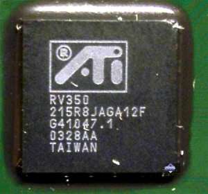 On the threshold of October ATI Technologies announced its Radeon 9800XT and Radeon 9600XT that were essentially the variants of Radeon 9800 Pro and Radeon 9600 Pro, respectively, with increased clock speeds. Both novelties were made by Taiwanese TSMC. Radeon 9600XT with its 0.13µm process and 500/600 MHz DDR clock speeds remained the most modern solution. And TSMC's 0.13µm process also included the new Black Diamond low-k dielectric from Applied Materials. 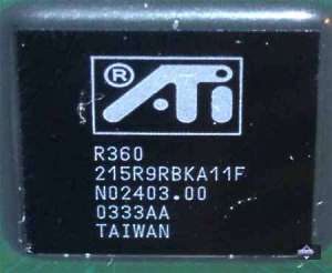 Unlike Radeon 9600XT, ATI's top-end Radeon 9800XT (R360) was still made using the older 0.15µm TSMC process. To raise its clock speed up to 412 MHz (almost by 15% comparing to Radeon 9800 Pro) they had to optimize GPU metallic layers layout, memory controller, PCB design and cooling system. 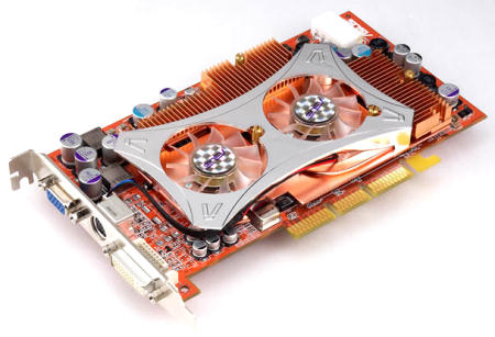 So, 9800 XT based on the newly designed PCB and had a new larger copper cooler that still didn't occupy the neighbouring slot. And NVIDIA had some problems in the beginning of the year. The expensive and not the most stable GeForce FX 5800 Ultra (later even called unsuccessful by NVIDIA itself), was crowned the top until May, when we saw the new GeForce FX 5900 / 5900 Ultra GPUs to replace GeForce FX 5800 and GeForce FX 5800 Ultra. The GF FX 5800 series was excluded from the roadmap and the first offspring of 0.13µm technology was replaced by NV35. I guess one of the primary reasons of GeForce FX 5800 failure was its memory interface just 128-bit wide designed for rather problematic and fast DDR2. Other features of NV35 includes 0.13µm process technology, up to 450 MHz GPU clock, 256-bit memory operating at 425 MHz, up to 256 MB DDR/DDR2 support. Naturally, the new processors have doubled memory bus width compared to GF FX 5800 providing bandwidth up to 27.2GB/s (vs. the previous 16GB/s). Besides, the new GPU generation obtained the improved High-Resolution Compression (HCT) technology for 256-bit memory - Intellisample HCT, and the new CineFX 2.0 engine supporting UltraShadow shadows and lighting rendering acceleration technology. Earlier in March NVIDIA updated its GeForce FX series with two DirectX 9.0 GPUs, GeForce FX 5600 and 5200 for performance and mainstream markets. Each supports CineFX, pixel and vertex shaders, but features only 4 texture units. In May the company launched the new stepping of NVIDIA GeForce FX 5600 working at 400 MHz and supporting 400 MHz memory. The production of GeForce FX 5600 (NV31) was at the beginning based on the 0.13µm process. The GPU features 88 million transistors and supports DDR-2 and all GeForce FX technologies, including Intellisample 2.0. Cards on this chip usually have 128 MB 128-bit DDR and operate at 325/275 MHz. GeForce FX 5200 (NV34) was company's first mainstream DirectX 9.0 GPU positioned at the level below $100. It's made using 0.15µm process and has 81 million transistors, supports only DDR-I. Initially they planned mainly 128 MB 128-bit DDR versions, but actually released 64/128 MB 64-bit models as well. 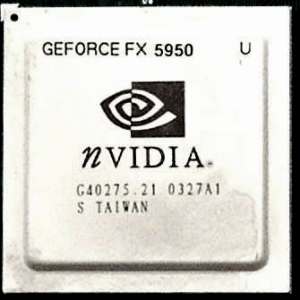
Closer to the end of 2003, late in October, NVIDIA informed on the release of its new GeForce FX 5950 Ultra and GeForce FX 5700 GPUs. Made by TSMC using 0.13µm process, NVIDIA's most powerful GeForce FX 5950 Ultra (NV38) has 475/950 MHz GPU/memory clock speeds, supports 256-bit memory, and is a natural successor to GeForce FX 5900. At the same time its halved variant, NVIDIA GeForce FX 5700 Ultra (NV36) GPU, operating and 475/900 MHz is the first GPU made by IBM using 0.13µm process. 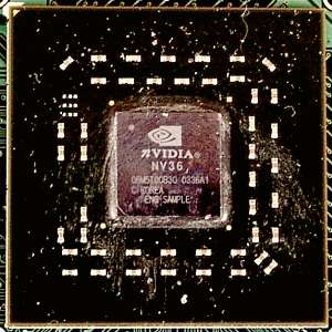 The GeForce FX 5700 series that also includes GeForce FX 5700 (NV36 at 425/550 MHz) supports DirectX 9.0 and represents the middle-level performance solutions. Finally, there's GeForce FX 5600XT, a variant of NV31 (FX 5600), on simpler PCB clocked at 230/400 MHz. 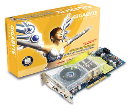 It seems that the largest event of PC graphics market in 2004 will be the transition to PCI Express 16x. It's not a secret that already by the mid-2004 PCI Express 16x is forecasted to become a common-purpose interface (not dedicated to graphics only like AGP) in the majority of the new desktop motherboards. Let's try to sum up the advantages of moving to PCI-Express for a typical desktop system:
The first PCI Express motherboards will have 1 x PCI Express 16õ slot primarily for graphics cards. In H1 2004 we should see the first PCI Express solutions from NVIDIA (NV40/41/45, etc. as well as the new PCI-Express version of NV36-NV36Õ) and ATI (R420, etc.)  The next generation of NVIDIA solutions will base on NV40 (TBA Spring 2004, according to the recent information on NV40 development and sample production), mainstream NV41 (TBA 2-3 months later as usual), and perhaps some other cheaper models (NV42/43) repeatedly rumoured about that might represent original NV41 with somehow blocked features. In a half-year after the announcement of NV40 or even later we should expect its improved variant, NV45, more powerful and more mainstream, and, of course, another number of cheaper solutions (NV46, etc.) ATI, in its turn, plans to release its R420 GPU in Spring that took much to the successful R300. Of course, it's promised to be considerably more powerful. The natural mainstream model will be the RV420. The next ATI architecture codenamed R500 should be announced later, perhaps in the Autumn 2004. We also know that ATI plans to release two variants of its new GPUs for AGP 8x and PCI-Express 16x buses, and is even going to announce PCI-Express 16x version of mainstream RV360 (380). NVIDIA also plans to release an inexpensive PCI-Express 16x solution, NV38X initially called to occupy the place for mainstream NV41/42/43. However, NVIDIA's approach to AGP cards on NV4X is not clear. One piece of information states that they'll have APG to PCI-Express bridge chips, another piece claims they'll have both interfaces. And now the most interesting - the performance. Both rivals will make their new series using0.13µm processes (with some improvements compared to the basic ones used for NV30 and RV350, respectively). Perhaps, NV40 will be made at IBM's fab like the already successful NV38. And, perhaps, NVIDIA will use both available production facilities and share various NV40 orders between TSMC and IBM. ATI is still works only with TSMC, but this might also change with time. In Spring the key role will play the 600 MHz graphics memory that will limit the clock speeds of ATI's and NVIDIA's top-end GPUs. The final clock specs will be defined just before the announcement (actual statistics is required), but we assume they won't exceed 650 MHz and get below 500 MHz for NVIDIA. ATI, in its turn, due to the architecture peculiarities will, most likely, aim at 500-550 MHz. But it's hard to be specific here as the company is on the brink of transition to 0.13µm. It's logical to await the support of pixel and vertex shaders 3.0 from both makers. The performance payoff for the implementation is not clear yet for both NVIDIA, and ATI. But the specs assure these will be supported anyway. The number of texture units will, most likely, be doubled by NVIDIA and ATI, though considering the significant architectural pixel shader advantage of the latter, we might expect something less radical like 12 texture units and pixel pipelines in R420. This time the main limiting factors in real apps will be the clock speed and memory. From the angle of top performance, I can forecast the approximately doubled values for pixel shaders of NV40 compared to NV35 and slightly less than double for R420 compared to R350. However, the most interesting battles are expected in the mainstream segment: there are rumours that the fashion of "halving" senior models to obtain mainstream is passed, so RV420 and NV41 will be more powerful than we think they will. Well, only the time will tell. Let me finish by observing the symptomatic and most likely trendlike situation with Taiwanese graphics card makers. From times immemorial a certain manufacturer was actually considered "attached" to either GPU vendor, and the change for another was accompanied with the existing contract loss and partnership breach. Of course, often it didn't touch the OEM shipments to large retailers. But this latter also didn't imply any manufacturer support or the newest GPUs. In September ASUS, for the first time in the latest history of business, changed this situation by signing a contract with ATI and simultaneously remaining a good partner of NVIDIA. The proof is the graphics card releases on the latest GPUs from both ATI and NVIDIA. Another large Taiwanese maker, Gigabyte, followed ASUS, and I assume this might become a natural trend. At the same time, according to the messages from Taiwan, both companies might also like to release products on XGI GPUs. Well, let's just hope that such "3D pluralism" will benefit the end user. Besides, I can't miss two key trends formed in in 2003. First is implementing thermal sensors into GPUs for automatic performance management. It's not the worldwide fashion at the moment, but the fact of "borrowing" ideas from CPU makers is clear. Another noticeable trend is the integration of an additional power connector witnessed in not only the top-end, but also middle-end solutions. Write a comment below. No registration needed!
|
Platform · Video · Multimedia · Mobile · Other || About us & Privacy policy · Twitter · Facebook Copyright © Byrds Research & Publishing, Ltd., 1997–2011. All rights reserved. | |||||||||||||||||||||||||||||||||||||||||||||||||||||||||||||||||||||||||||||||||||||||||||||||||||||||||||||||||||||||||||||||||||||||||||||||||||||||||||||||||||||||||||||||||||