|
||
|
||
| ||
|
||
|
||
| ||
Manufacture, technologies, tools Litho market, suffered most during past two years, is at last expected to get better in 2003. According to Information Network analysts, in 2003 litho shipments are expected to make $4.3 billion or 547 tools, or 25.6% industry growth. Chip makers will be most interested in new 193 nm for 90-nm production lines. Besides, next year 248-nm tools for 130-nm process are expected to start leaving the market. Having touched new litho tools, it's worth remembering the results of October International EUV Symposium, where both current implementation problems and future prospects were discussed. As you know, R&D works for implementing modern litho tools cost very much. One of latest trends is the creation of various R&D centers for several companies at once to develop new technologies together. Naturally, investments into such cooperative projects costs less for the participants. What's even more interesting on this background: on the wave of future EUV (extreme-ultraviolet) tools development, state institutions pay more and more attention to such works. This is most noticeable in Europe, Japan, and USA. International EUV Lithography Symposium brought the following: in USA federal investments into EUV development will be provided by DARPA (Defense Advanced Research Projects Agency) and National Institute of Standards and Technology. Separately, New York promised to spend about $280 million within the next 5 years for EUV photoresists and photomasks center in Albany. These years European Union countries plan to spend about $100 million for various EUV projects. For example, between 2001 and 2004, Germany is to spend about $50 million for R&D works on EUV components: lasers, mirrors, photomask substrates, metrological tools, etc. In general, expenses of German companies are expected to be 40% compensated by the government. Currently, according to various sources, total worldwide EUV investments exceeded cymmy $1 billion. Another several billions are to be spend by the moment when EUV scanner production makes 100 plants/year and expenses start to be repaid. In his speech Peter Silverman, Intel's director of lithography capital equipment and one of the members of International EUV Symposium, shared his thoughts about EUV tools implementation prospects.
Generally, specialists outlined three most important problems of EUV lithography implementation:
Another important problems include reduction of EUV photoresist cost price, plant thermal stabilization and environmental pollution control. To sum up our brief EUV digest, I'll mark that not all companies agree with Intel about EUV beta plants in 2005 and volume-production of EUV scanners in 2007. Sceptic Texas Instruments shift the release of beta plants to 2007, commercial EUV systems - to 2009 or 2010. Due to this, not rejecting the participation in EUV system development, TI also bets on combined usage of ASML 157 nm scanners and Nikon's projection electron beam lithography (EPL). TI already ordered three C20 157 nm scanners from Dutch ASML and plans to get as close as possible to 65 nm chip production at the new 300-mm DMOS 6 fab within 2 years. In other words, opinions vary. Only time will tell, if financial problems can move commercial EUV litho tools to the end of the decade. However, the serious approach to the problem and considerable sums, spent for R&D, enable to think that problems will be solved according to the schedule. As the current problems do not go against fundamental physics and are mostly technical. But let's get back from the future to the current time and remember some important industry events. According to the schedule, Intel announced the grand opening of new Fab 11X in Rio Rancho, N.M. for making semiconductor products on 300-mm wafers. $2 billion fab is initially built for 300-mm volume production using 0.13-micron process technology. In 2003 Fab 11X is planned to transit to 0.09-micron process. The Fab size is over 1 million square feet in size. Clean room space makes about 200,000 square feet.  Another tendentious October event is the creation of R&D alliance of Intel and eleven Asian portable PC makers. Now Intel won't only ship new chips to the partners, but also develop ready solutions together with them. The alliance, including Quanta, Samsung, LG Group, Hon Hai Precision Industries, Wistron, Compal Electronics, First International Computer, Inventec, Asustek, Gigabyte, Micro-Star International, and Mitac International, will research ways for increasing notebook battery operation, system performance, reducing form-factors, and integrating wireless connectivity. First alliance products are expected in 2003. According to Intel, one of the reasons to create an alliance was that Asian companies provide 60% of worldwide notebook shipments and more than 75% of worldwide mobo shipments. In October Hitachi and Mitsubishi decided to join some of their subsidiaries to cut expenses and increase profitability. The new Renesas Technology with 50 billion yens ($410 million) starting capital will be formed in April 2003. Hitachi's share will be 55%. Besides, Hitachi and NEC reported that their Elpida Memory joint venture decided to purchase Mitsubishi Electric DRAM production department. Past month IBM created new IBM Engineering & Technology Services department, that will focus on four main services: business solutions (manufacture optimization; e-design, including certification and web hosting; manufacture renewal, technology migration (including migration to SOI) consultations), technological optimizations (silicon wafer, chip, integrated array production; development of alternative power supply technologies and frequency ranges; yield analysis; chip, module, board modelling optimizations), system solutions (development of platforms and components; system-level optimizations; software and hardware testing), technological outsourcing (semiconductor production; complete chip and system solution development and production services). First customers of IBM Engineering & Technology Services will include Minolta and Sony Computer Entertainment (SCE). SCE ordered comm chips for PlayStation2. Minolta requested the development and production of control elements for office combo products. ProcessorsOctober was more than rich with processors, it's even too much for this digest to mention all of them. For the sake of justice I must admit the announcements were more of a declaration than practical. It's no surprise, as this month hosted Microprocessor Forum, that brought many prospects of various companies at least for a year. Let's start with AMD products. Excluding AMD Athlon XP 2800+ and 2700+ with 333 MHz FSB, announced early in October, there were no messages from AMD about new processor releases. We've already described AMD Athlon XP 2800+ and 2700+ in the previous digest. The month has passed and AMD 333 MHz FSB announcements turned out to be "paper only". There were no messages about Athlon XP 2800+ and 2700+ seen in retail. Moreover, Athlon 2400+, announced earlier, hasn't become widespread as well. At the quarterly press conference company announced the intention to release about 2 million of such chips in Q4. 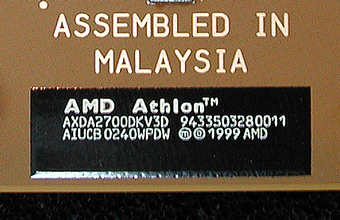 Despite repeating quarterly losses, the company seriously strives to restore desktop PC market positions and enter the server processor market. Moreover. Strategy changes, announced at Q3 results conference touched exactly the server CPU market. It seems that now release of Hammer server version - Opteron becomes one of the top-priority company aims. The announcement of first desktop Hammers is now somewhere in Q1/Q2 2003. Barton-based Athlon XP is still expected in Q1 along with server and workstation Barton MP. At Microprocessor Forum AMD showed samples of 2 GHz 64-bit Opteron with 1MB L2 cache along with performance results: in 32-bit mode with PC2700 DDR SPECint base2000 indicated 1202 and SPECfp base2000 - 1170. these are significant values, but let's wait for serial models. In October Intel caused many more processor news. The most anticipated news is about Banias products, expected in mass quantities in several months. In October Intel also paid serious attention to Banias seminars - during Intel Developer Forum in Taipei and Tokyo, at MPF 2002 (Microprocessor Forum). The burden was "Banias is at hand". From declarations Intel turned to the demonstration of actual prototypes and comprehensive presentation of their technical specifications. It's already known that first Banias will have 1MB L2 cache, up to 1.6 GHz clocks. Observers believe that Banias release will become one of the most important events of the next year. Initially designed for ultra light and thin notebooks Banias is aimed at all mobile PC market segments from business class to tablets.
The announcement of new Intel Xscale processors turned complex due to chip design. New chips are based on system-in-a-package (SIP) technology, in its turn, based on multi-level-cell (MLC) packaging.  PXA261 and PXA262 processors feature XScale PXA250 RISC core and Intel StrataFlash memory. Intel's first SIP products feature chip-scale package (CSP) of 13x13x1 mm dimensions. Intel PXA261 features 200 MHz XScale PXA250 and 16MB flash memory. Intel PXA262 features 200 or 300 MHz core and 32MB flash memory. In October at Asia-Pacific Intel Developer Forum (APAC IDF) Fall 2002 Intel announced new Manitoba mobile processor, combining Xscale core, digital signal processor, and flash memory. Commercialization is expected next year. Supposedly, Manitoba will debut in new 2.5G GSM/GPRS phones. According to the company, Manitoba processors are currently made using 0.13-micron process, however already in 2003 the production will be moved to 0.09-micron process. In October Intel also announced new 400 MHz Ultra Low Voltage Celeron for embedded systems - storage devices, industrial PCs, etc. The new chip dissipates nominal of 3.4W, up to 4.2W. It's designed for working together with Intel RadiSys 82600 chipset, base for RadiSys EPC-6315 mobo for embedded systems. The chip can also be used with Intel 440MX and Intel 815E systems. New 400 MHz Ultra Low Voltage Celeron features 256 Kb L2 cache, supports 100 MHz FSB, and is made using 0.13-micron process technology in ÞFCBGA package. Core voltage makes 0.95V, temperature range is 0°C to +1000°C. I'll finish with Intel October novelties with new IXP2850 chip on Intel IXP2800 programmable network processor architecture. It's designed for comm devices and can be programmed for load-balancing, etc. Besides, the chip has hardware support of encryption and data integrity - 3DES, AES, SHA-1 - at up to 10 Gbps throughput. Intel IXP2850 is compatible with the existing IXDP2800 hardware development platform. The existing Intel Internet Exchange Architecture (IXA) Software Development Kit 3.0 was changed to support new security features and cut maintain costs. In October VIA Technologies has also showed activity and reported not only about new processors and prospects, but also about closest chip releases. For example, after VTF 2002 and Microprocessor Forum 2002 we received information that 1 GHz C3 has been excluded from the roadmap for good. Now C3 line ends with 933 MHz chip. 1 GHz C3 is replaced by Nehemiah (C5XL) processor. VIA is to ship its 1 GHz samples in Q4 2002. The new Nehemiah (C5XL) core is not something ultra new, featuring architecture already known by C3 (C5N and Ezra-T). Still the core has changed significantly: 17 pipeline stages instead of 12, SSE support, x87 floating point block, operating at full clock. In other words, the same architecture, but honed and shaped up. According to company representatives, C5XL core will contain 32% more transistors then the current C5N, however, the crystal size is reduced from 56 to 52 sq.mm. VIA plans to leave the cost price at the same level, if not to reduce it as well. In 2003 VIA plans to raise chip clock to 1.4-1.5 GHz. 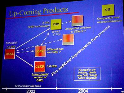 Now in the end of 2003 / beginning of 2004 the company plans to release C5Z core, a higher performance version of C5X, featuring about 2GHz clocks, 22-stage pipeline, SSE2 support, 80 sq.mm crystal, 0.13-micron process. For the low-end market the company plans to release low-power C5XP core and also C5Y with a new high-performance bus. Integrated C5XL and C5Z are planned to 2004, and further plans indicate a mysterious CN chip (perhaps, "N" is a place for another digit) with a completely new architecture. VIA's ESP processors for the Eden platform are expected to reach 1GHz and higher (currently there are ESP4000, ESP5000, and ESP6000 chips, featuring 400MHz, 533MHz, 667MHz clocks, respectively). Now the company prepares to release ESP8000 and ESP10K with 800MHz and 1GHz, respectively. ESP8000 is expected to feature Nehemiah core, next generation after VIA C3.ESP10K will feature the next generation core (Esther?) after Nehemiah, supporting SSE/SSE2 (FYI: ESP8000 will only support SSE). ESP8000 is expected to appear in November, volume shipments are scheduled to Q1 2003. ESP10K will be announced in Q3 2003, volume shipments will begin in Q4 2003. According to provisional data, ESP8000 / ESP10K will require up to 6W/8W. At Microprocessor Forum IBM announced the first 64-bit PowerPC. Featuring 1.8 GHz clock and supporting Altivec instructions for multimedia data processing and operation in up to 16-unit systems, it will become the base for new Apple Macintosh computers, that might appear in the market late next year. 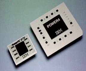 PowerPC 970 32/64-bit architecture is realized rather simply: a special instruction flag enables 32-bit mode and upper instruction and data bits are ignored. Both 32/64-bit modes feature 8 instructions per cycle. Besides, all 32-bit PowerPC specifications have remained the same. At the same time 64-bit addressing, similar to AMD Hammer, will enable to migrate to 64-bit OS and apps. But enable whom? Industrial sources claim that PowerPC 970 can be well used in Apple's next-generation systems. Apple Computer has been interested in 64-bit processors for a long time. Besides, 64-bit computing advantages, in case the company continues to work together with IBM it will get 1.8 GHz PowerPC 970 already in 2003. Moreover, IBM plans to quickly reach 2 GHz limit and announce lower-power chips for notebooks. Naturally Apple (a company that loves surprises) is traditionally silent about such claims. First, PowerPC 970 will be made at IBM's fab in East Fishkill, NY, using 0.13-micron process and SOI. In H2 2003 IBM plans to migrate the production to 90 nm. At Microprocessor Forum English ARM announced two new ARM1136J-S and ARM1136JF-S processor cores. The new chips are the first products with ARM11 processor architecture, first announced in April at Embedded Processor Forum. Both support ARMv6 instruction set. ARM1136J-S and ARM1136JF-S are designed for a wide variety of consumer electronics, wireless, comm devices: consoles, digital cameras, 2.5/3G mobiles, VoIP tools, broadband modems, WLAN access points, etc. New ARM11 chips, already offered for licensing, feature 533 MHz and higher clocks and will be made using 0.13-micron process technology. Their performance is estimated 600 Dhrystone MIPs (w/o optimizations) at up to 200 mW power consumption. Typical power consumption of 0.13-micron ARM1136J-S and ARM1136JF-S at 400 MHz, 1V voltage makes 160 mW. Chips feature 8-stage pipeline with 2-cycle cache, enabling to raise clocks in the future. Both feature flexible high-performance memory engine with programmable instruction set, data cache, and TCM DMA memory for real-time data processing. Memory management unit (MMU) is supported by Microsoft, Symbian, WindRiver, and Linux. Chips feature four 64-bit ports, connected to the memory controller, support 32-bit DDR, and feature 32-bit peripheral bus. The letter F in ARM1136JF-S marking means built-in floating-point coprocessor. Both cores support ARM Jazelle extensions for faster Java processing, and ARM "E" extensions for DSP optimization. Both cores are supported by ARM RealView, featuring RealView Compilation Tools, RealView Debugger, Multi-ICE, RealView ICE, and RealViewTrace. Samsung Electronics' Halla is another new ARM core for embedded apps, that's pin-compatible with popular ARM1020E, but claimed to have more advanced features even comparing with Intel XScale. In particular, chip initial clock is great - over 1.2 GHz. Samsung plans to use Halla in its Pocket-PC and digital TV chips. According to Samsung, they've considered Alpha developments while creating the core and this enabled such a serious clock increase. Samsung engineers completely redesigned the core and circuitry, using dynamic nodes with dual-channel buses and low-amplitude signal for time-critical parts. Besides, control logic has been redesigned as well. Halla samples are expected in Q2 2003. They'll be made using 0.13-micron process technology, enabling to reduce 1.2 GHz chip energy consumption to 1.8W, 800 MHz chip energy consumption - to 550mW.
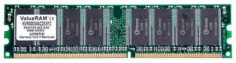
Motherboards and chipsetsThe central and naturally the most anticipated in October was the official release of 4 new Pentium 4 desktop chipsets by Intel. Besides, three expected - 845GE, 845PE, 845GV - Intel also announced the "enhanced" 850E. All the new chipsets support Hyper-Threading (HT) for the software dual-chip modelling with one physical. According to the official statement, HT will be supported by desktop processors later, with the release of 3.06 GHz Pentium 4. As for the enhanced 850E, it now officially supports PC1066 RDRAM. New discrete 845PE and integrated 845GE differ from their predecessors - 845E and 845G - by DDR333 support. You can read more about these chipsets and motherboard performance from the Latest Intel Pentium 4 chipsets review about Intel 845PE, Intel 845GE, SiS648, and VIA P4X400 boards. New integrated Intel 845GV, to replace budget 845GL, will now support Pentium 4 and Celeron, though officially it can work with up to DDR266 only. Along with the release of new chipsets, Intel announced 6 new motherboards: ATX D845GEBV2 (on the photo), D845PEBT2, D845PESV, D850EMVR, and also micro-ATX D845GERG2, D845GVAD2. 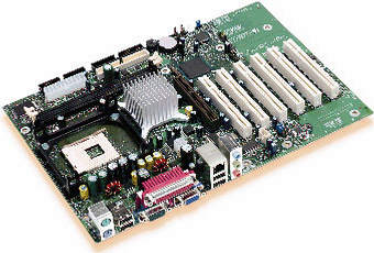 They are not extraordinary, but good. Besides, all the companies released 845GE, 845PE, 845GV novelties, having been announcing their specs already in September. Naturally, the release of new DDR333 logic will additionally boost mobo and system memory market. in the future it might result in strengthening DDR SDRAM position, and maybe to Intel's domination on P4 chipset market. October also brought Intel Plumas or E7500 boards. ABIT announced the new dual-CPU SI-2Pa Xeon server board, based on this chipset. 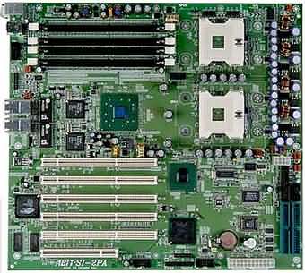 The board supports up to 2 Xeons with up to 2.8 GHz clock and 512KB L2 cache, features Intel E7500 (Plumas 533) MCH, Intel 82801CA I/O Controller Hub 3-S (ICH3-S), Intel 82870P2 64-bit PCI/PCI-X Controller Hub 2 (P64H2), 4 DIMM sockets, up to 8GB registered DDR200/266 w/ECC, Five 64-bit PCI-X slots, 32-bit / 33MHz PCI slot, 2 dual-port Gigabit Ethernet controllers Intel 82546EB (Anvik), 4 Gigabit Ethernet LAN ports, Integrated ATI RAGE XL PCI graphics, 4MB SDRAM, 2 USB ports, Smart Card port, EEB 3.0 form-factor. In October SuperMicro announced new P4DPL-M server board on Intel E7500 chipset, supporting up to 2 Hyper-Threading-enabled Intel Xeon with 400MHz FSB and up to 2.80 GHz clocks. P4DPL-M supports up to 12GB PC1600 SDRAM, features one 133 MHz and 100 MHz PCI-X slots, three 33 MHz PCI slots, ATI Rage XL (8MB, PCI) integrated graphics, 10/100 Fast Ethernet (Intel 82551). In the near future the company is also to announce - P4DPL-8GM and P4DPL-iGM, based on P4DPL-M, with additional features. P4DPL-8GM will have dual-channel Ultra320 SCSI controller, supporting Zero channel RAID, Gigabit Ethernet and IPMI 1.5. P4DPL-iGM will differ from P4DPL-M by a Gigabit Ethernet port and IPMI 1.5 support. VIA KT400 remains the leader among AMD K7 chipsets both in shipments, and new board releases. If VIA reported about KT333 chipset deficit in Q3 due to increased demand, in October the company mentioned the lack of KT400. This time the deficit was caused by the lack of materials due to unambiguous economical situation, observed earlier. Mobo vendors noted the considerable increase of motherboard demand, though it's usual for the fourth quarter. Due to the increased demand and shipments, respectively, VIA forecasted the October revenues to be higher than in September. Though in November the company expects lower sales volumes similar to September. Due to AMD K8 release delay, VIA and SiS are going to prepare for new K7 releases - KT400A and SiS746FX. As AGP 8x and DDR333 are already supported by KT400 and SiS746, new chipsets will, most likely, support DDR400. Having recently entered the market, NVIDIA started to push traditional leaders aside. In October it announced 35% presence on the AMD K7 OEM market, mainly due to orders from Sony and Compaq Computer. NVIDIA plans to strengthen its position in the clone sector by improving products' price/performance. The nForce2 chipsets will support DDR, Dynamic Adaptive Speculative Pre-processor (DASP) technology and 333MHz FSB, and will not cost higher than comparable products from competitors. In addition to the desktop clone market NVIDIA has also decided to introduce core logic chipsets into the notebook market in 2003. ABIT NV7-8X became one of the October boards on NVIDIA nForce2 SPP + MCP2-T bundle.  The board features ATX design, and bases on NVIDIA nForce2 SPP + MCP2-T chipset bundle. It supports Socket A Duron/Athlon/Athlon XP with 200/266/333 MHz FSB, has AGP 8È slot, 3 DIMM sockets (up to 3GB DDR 200/266/333 or up to 2GB (in two sockets) DDR 400), 5 PCI slots, 2-port Serial ATA interface, 6-channel audio codec, 24-bit S/PDIF, integrated 10/100Mb LAN, IEEE 1394, and USB 2.0 ports. October brought the first messages about new ASRock, initially the subsidiary of ASUS. Can't specify any release dates, however, the boards are expected to differ by aggressive pricing. Most of them will be based on SiS chipsets. Memory productsI guess the most interesting memory market events of October were about JEDEX Beijing, that took place in Peking. JEDEC continued drafting an addendum to the DDR-II standard that would cover 2Gbit chips expected in 2005. DDR-II specs also has been amended to double the number of memory banks to eight for 1Gbit and higher-capacity chips. The increased number of banks reduces latency and boosts memory chip efficiency. All DDR-II memory modules will use new BGA packaging because of its smaller form factor. JEDEX brought the first info about draft specs of next-generation DDR-III SDRAM. These very provisional DDR-III SDRAM features include 800 Mbps throughput with consequent increase to 1.5 Gbps. DDR-III power requirements will also be different, making 1.2V or 1.5V (against 1.8V of DDR-II and 2.5V of the current DDR). According to Infineon Technologies, typical capacity of the first DDR-III SDRAM chips will make 4 Gbit. DDR-III is expected to feature short-loop through (SLT), the signaling technique, also used in some DDR-II devices to reduce noise at high frequencies. JEDEC will approve final DDR-III specs closer to the end of 2005 along with the first appearance of samples. DDR-III volume production is expected in 2007. According to JEDEC sources, five DRAM makers, including Elpida, Hynix, Infineon, Micron, and Samsung, decided to share main parts of the future standard to develop draft specs independently and presumably join them at December quarterly meeting. The central place in messages from JEDEX Beijing was taken by DDR-II development body. It has even caused some mess with names of the future standard. According to Micron Technology, the difference in ATI GDDR3 and NVIDIA GDDR-2 specs is that NVIDIA implemented 1Gbps linear throughput, and ATI specs feature 1.4 Gbps transfers. This 40% additional performance made ATI call its standard GDDR3. Though this naming problem will be solved very soon - in December. By that time the committee should come to a consensus about the name and will announce the final specifications. New graphics memory specs define key changes in frequency determining circuit and I/O interface design, better suited for point-to-point graphics controller architecture. Exactly this data transfer method makes DDR-II differ from system DRAM. Micron representatives promise to launch GDDR-II volume production already in Q2 2003, Korean Hynix Semiconductor - in H1 2003, Infineon Technologies plans to announce samples in H1 2003 as well to launch volume production later. Initially graphics DDR-II modules are expected to feature 256 Mbit capacity, 500 MHz clock and 1Gbps linear throughput. Despite the specs are based on DDR-II standard, these will be completely different CSP (chip-scale packaging) chips of 144-pin BGA configuration unlike 84-pin DDR-II CSP chips. In October Micron finished the development of 533 MHz DDR-II chips. By doing this it joined Samsung and Elpida Memory, and has become the third vendor, ready to commercialize DDR-II production. Samsung announced its 512 Mbit DDR-II chips as far back as in May. Elpida Memory finished the development of similar product in July. Hynix Semiconductor hasn't yet announced any DDR-II samples, but is going to outrun rivals technologically. In October the company announced 512 Mbit DDR SDRAM samples, made using 0.10-micron process. New 512 Mbit DDR SDRAM chips are claimed to be compatible with DDR 266, DDR 333, and DDR 400. New high-precision process was launched at three fabs in Korea and USA. Hynix plans to launch volume production of new 512 Mbit DDR SDRAM later this year. 0.10-micron 256 Mbit and 1 Gbit DDR SDRAM is scheduled to H1 2003. Now something about more actual memory. Kingston Technology announced new 256MB and 512MB PC3200 (DDR400) memory modules under its ValueRAM brand. New Kingston's modules were tested on the Agilent 83000 platform and in current DDR400-enabled chipsets. Kingston will release the following modules: KVR400X64C25/256 256MB 400MHz DDR DIMM, CL 2.5; KVR400X64C25/512 512MB 400MHz DDR DIMM, CL 2.5. They are expected in Q4 2002. 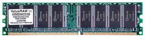
 Canadian Corsair Memory announced two DDR DRAM modules, XMS3500 series - eXtreme Memory Speed ("XMS"). The first one, Corsair CMX512-3500C2 is a 512 MB module supporting 434 MHz, CAS (Column Access Strobe ) = 2.0. The second - CMX256A-3500C2 - is 256 MB in capacity and similar specs. 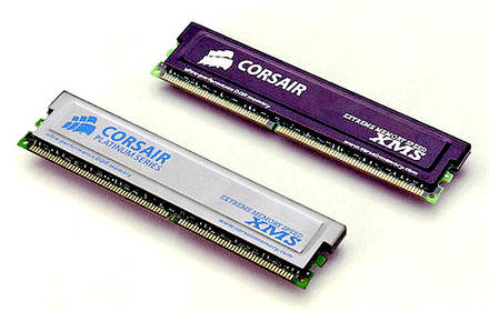 CMX256A-3500C2 are based on the same 5 ns 32M x 8 DDR SDRAM chips, as featured in CMX512-3500C2. They are shipped with black or platinum aluminium heat-sinks. Very late in October Japanese Melco announced new 16- and 32-bit RDRAM PC1066 and DDR SDRAM PC2700. RD1G is a 16-bit RIMM PC1066 module (tRAC=32 ns), sold in two-unit packages. 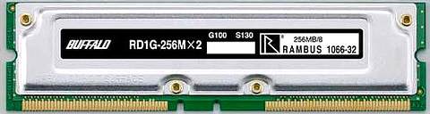 RD1GW represents 32-bit RIMM PC1066 (tRAC=32 ns). They are sold apiece, 256MB module costs about $200, 512MB module - about $390. 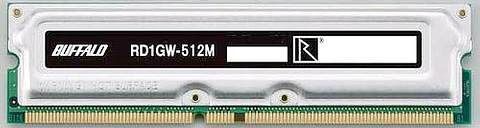 New DD333 series of PC2700 DDR SDRAM (SPD, CAS=2.5) includes 128MB, 256MB, 512MB modules.  In October Intel announced new 1.8V StrataFlash Wireless Memory samples, made using 0.13-micron process technology (such memory is used in new integrated Xscale processors). The previous StrataFlash generation required 3.3V voltage and was made using 0.18-micron process. New 64, 128, and 256 Mbit StrataFlash are to appear in the market in Q2 2003. 128 Mbit samples are available now for $17.75 in over 10,000-unit quantities. 64 Mbit and 256 Mbit chips are to appear early in 2003. AMD announced new 16 Mbit chips - Am29BDD160 - for automotive environments, including power-train management, high-end engine control modules, and Anti-lock Brake Systems (ABS). According to AMD, they are industry only flash modules with 66 MHz clock and -40°C to +145°C working temperature range. Am29BDD160 chips support Simultaneous Read/Write, have interface for industry-standard microprocessors including Motorola MPC, Infineon Tri-Core, and Hitachi SH-4 series microcontrollers, and support Advanced sector protection architecture. Volume production is expected late in Q4 2002. In October Fujitsu announced the development of new memory chips, including 6 chips of various purpose, packed into single Package Stacked Multi Chip Package (PS-MCP). MB84VY6A4A1 have 179-pin BGA and are sized similar to the current 4-chip Fujitsu products - 15x11x1.4 mm. At that their capacity is 20% higher. A chip includes three 128 Mbit NOR memories with page mode support, two 64 Mbit FCRAM, and one 8 Mbit SRAM. Fujitsu plans to produce new 6-chip products early in November. They'll be mainly intended for the mobile and PDA markets. By Vladimir Romanchenko (lone@ixbt.com)
Write a comment below. No registration needed!
|
Platform · Video · Multimedia · Mobile · Other || About us & Privacy policy · Twitter · Facebook Copyright © Byrds Research & Publishing, Ltd., 1997–2011. All rights reserved. |