 |
||
|
||
| ||
|
||
|
||
| ||
A new generation of desktop/mobile processors VIA C7/C7-M was presented by VIA Technologies relatively recently — in the end of May - beginning of June 2005. Nevertheless, these processors appeared in ready solutions (notebooks, as well as pc1000/pc1500 platforms) much later. There is still no technical documentation on these processors (unlike the previous model — VIA C3), the main official information is published only on the manufacturer's web site. So, the new generation of VIA C7/C7-M processors (they differ mostly in their titles and maximum clocks) uses the Esther core, based on the VIA CoolStream(tm) architecture. Philosophy of this architecture is based on three components — Secure by Design, Low Power by Design, and Performance by Design. The first component is provided by the traditional VIA PadLock module, built into the core, which was supplemented in these processors with SHA-1 and SHA-256 hashing and hardware support for Montgomery multiplier, used in RSA encryption algorithm, as well as NX (No Execute) bit. The second CoolStream component is achieved due to the 90nm SOI process technology from IBM. In this connection, power consumption of C7/C7-M processors amounts to just 12-20 Watts (depending on a clock — from 1.5 to 2.0 GHz, correspondingly). The third component (performance) is provided by the VIA StepAhead(tm) technology, consisting in VIA V4 bus (P4 Quad-Pumped bus counterpart) at up to 200 MHz (800 MHz quad-pumped), 16-stage pipeline, full-speed 128KB exclusive L2 Cache, and an improved branch prediction unit, typical of VIA. The second important factor of the third component is VIA TwinTurbo(tm), which allows a processor to switch between full-speed and power saving modes for one(!) CPU cycle thanks to two PLL units in a processor. Users of VIA C7/C7-M-based platforms cannot see the latter in action (to be more exact, VIA PowerSaver technology on the whole) — the manufacturer still hasn't developed an official CPU driver, which would allow an operating system to manage power consumption modes of these processors. Fortunately, we have found out experimentally that these technologies are implemented much better compared to their earlier version in VIA C3 — in full compliance with the well-known, one can even say standard, Enhanced Intel SpeedStep technology. Nevertheless, this article is not devoted to these technologies, it's about analyzing main low-level characteristics of the new Esther core in RightMark Memory Analyzer. We'll compare these characteristics with what we previously got for the VIA Antaur platform (mobile modification of the VIA C3 second generation with Nehemiah core, which was the first to support SSE instructions). Testbed configurationsTestbed 1 (Notebook MarcoPolo43T)
Testbed 2 (Notebook MaxSelect Optima C4)
CPUID CharacteristicsWe'll start examining the Esther core by the example of the 1.5 GHz VIA C7-M processor from analyzing the main CPUID characteristics. Table 1. VIA Antaur (Nehemiah) CPUID
Table 2. VIA C7-M (Esther) CPUID
Esther differs from Nehemiah very little in the main ID code — processor's signature: family number remains the same (6), only the model number was incremented by one (from 9 to 10). We shouldn't take a new stepping number seriously, as there may be several models differing in this parameter. However, we shouldn't have expected serious differences in family number (for example from Pentium II/III/M-like Family 6 to Pentium 4-like Family 15) — Esther can be considered an evolutionary step from Nehemiah core, like Yonah is an evolutionary step from Dothan. It is a direct analogy: Family Number remained the same (6), while Model Number was incremented by one (from 13 to 14), even despite dual cores in Yonah. At the same time, changes in the main low-level characteristics of Esther are quite serious. First of all it concerns L1-D/L1-I and L2 Caches of the processor — along with L2 Cache increased to 128 KB, its associativity has grown to 32(!), and lines sizes in each cache level have been increased to 64 bytes. Other changes include SSE2 and SSE3 instructions (the latter — without specific MONITOR and MWAIT instructions, which are relevant only for Intel processors with Hyper-Threading and/or multiple cores), as well as Thermal Monitor 1 (TM1), Thermal Monitor 2 (TM2), and Enhanced Intel SpeedStep (EIST). As we have already mentioned, the latter corresponds to the EIST-like implementation of the proprietary VIA PowerSaver technology. And finally, it's written in CPUID of C7/C7-M that these processors support NX bit technologies, mentioned above when we described VIA PadLock. Real Bandwidth of Data Cache/MemoryLet's proceed to analyzing test results. As usual, we'll start with the tests of real L1/L2 D-Cache and RAM bandwidth. 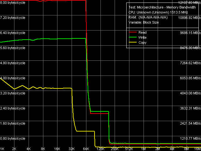
Picture 1. Real Bandwidth of L1/L2 Data Cache and Memory Bandwidth versus block size curves (Picture 1) look quite typical. We can say that the Esther core is characterized by exclusive L1/L2 Cache, L1 Cache size is 64 KB (the first inflection on read and write curves), and the total size of L1+L2 D-Caches is 192 KB (the second inflection). Table 3
Bandwidth ratings of all the three memory levels are published in Table 3. Compared to the previous solution from VIA — Nehemiah, Esther does not demonstrate evident advantages of its L1 D-Cache architecture. Its efficiency in reading data into MMX registers has grown. But at the same time, efficiency of write operations both from MMX as well as from SSE registers has gone down a little. In return, L1-L2 data bus has become more efficient (we are going to analyze it separately below), which manifests itself in higher L2 Cache efficiency both for reading and writing operations (in the latter case, L2 Cache bandwidth is even a tad higher than for reading, which is a rare phenomenon). Despite the faster 100 MHz V4 FSB (400 MHz Quad-Pumped), offering 3.2 GB/s theoretical bandwidth, as well as faster DDR-333 memory (maximum bandwidth - 2.67 GB/s), the real memory bandwidth for total reading (without optimizations) remains on a mediocre level - about 0.56 GB/s. At the same time, it's nice mentioning that this platform offers significantly higher memory bandwidth for writing data into memory — up to 0.62 GB/s. It's 3-4 times as high as on the earlier platform with a VIA Antaur processor. Maximum Real Memory BandwidthLet's evaluate the maximum real memory bandwidth using various optimizations. First of all, let's analyze software prefetch, which does very well with reading from memory for most modern processors. 
Picture 2. Maximum real memory bandwidth, Software Prefetch / Non-Temporal Store The curves of memory bandwidth versus PF distance (Picture 2) on a C7-M processor look noticeably different from the curves previously obtained on VIA C3/Antaur. In particular, the curves are characterized by a distinct PF efficiency maximum at the 192 byte distance (that is prefetching data 3 cache lines ahead of the current data), while software prefetch on C3/Antaur processors was not very efficient and memory bandwidth went down smoothly as the PF distance was increased. Maximum real memory bandwidth for this method (962 MB/s) is the absolute maximum — as you can see in Table 4, the other optimization methods are not so efficient. This parameter is also different from the previous generation of processors on Nehemiah core — in that case the maximum real memory bandwidth was achieved only using the "foul" method of reading whole cache lines (it's "foul" because this method cannot read all data from memory, though data transfer along FSB is done full-scale). 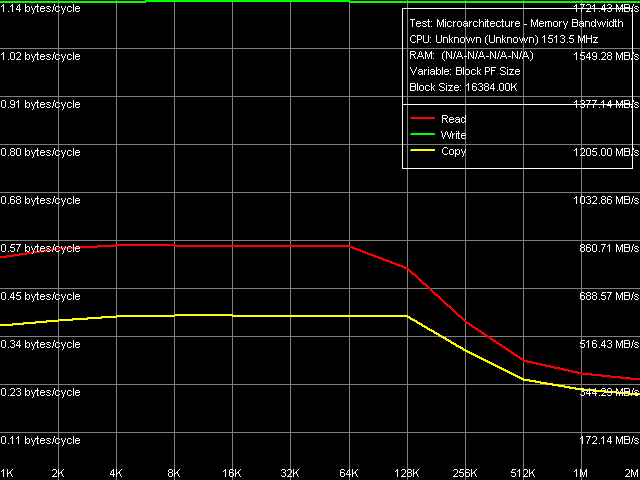
Picture 3. Maximum real memory bandwidth, Block Prefetch 1 / Non-Temporal Store 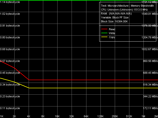
Picture 4. Maximum real memory bandwidth, Block Prefetch 2 / Non-Temporal Store What concerns Block Prefetch 1 and Block Prefetch 2 methods, the first one is initially designed for achieving maximum memory bandwidth on AMD K7 processors, the second method — for AMD K8, their behaviour on VIA C7-M (Pictures 2 and 3, correspondingly) is similar to what we saw on VIA C3/Antaur. Maximum efficiency of Method 1 is achieved at 64KB PF block, Method 2 — at 1KB (that is the second method is practically inefficient). And finally, the method of reading whole cache lines, which yielded the best results on VIA Antaur, is also quite efficient on C7-M (memory bandwidth — 910-920 MB/s). But its efficiency is a tad lower compared to software prefetch method. This layout of forces evidently favours the new Esther core, as Software Prefetch is the most frequently used, practically universal optimization method for reading data from memory. Table 4
What concerns optimization methods for writing data into memory, only one method is of real practical value — non-temporal store directly from MMX/SSE registers into memory via Write-Combining Buffers, avoiding the entire hierarchy of processor caches. It's also an ultimate leader on the early Nehemiah as well as on the new Esther platform — memory bandwidth on the latter reaches about 1.72 GB/s (Table 5), that is nearly 65% of the theoretical maximum. The method of writing whole cache lines, which yielded a tad larger memory bandwidth on Nehemiah, gives a surprise here — its efficiency is lower than that of the method of writing data through the entire hierarchy of processor caches. We cannot explain such behaviour. But nevertheless, it is of no great practical use, as this method is purely synthetic and cannot be used for writing real data into memory. Table 5
Average Latency of Data Cache/MemoryBefore we proceed to analyzing latencies of various memory levels, we'd like to remind you that the most significant change in D-Cache and I-Cache in new C7/C7-M processors with Esther core was increasing their line length from 32 to 64 bytes. As this very value appears in all latency tests and is determined automatically when RMMA starts on a new unknown processor, let's have a look at the curves of L1 and L2 D-Cache line sizes. 
Picture 5. Determining L1 D-Cache line size So, L1 D-Cache line size (Picture 5) does not admit of doubt — in all walk modes, maximum access latency increase in this test (which is a modification of the data arrival test) is demonstrated when reading a neighbouring element that is away from the main element by 64 bytes or more. Consequently, L1 Cache line size is indeed 64 bytes. 
Picture 6. Determining L2 D-Cache line size Quite a clear picture, but with some interference from hardware prefetch (yep, it was implemented for the first time in VIA processors, we shall see it in more detail below) is also demonstrated in the second L2-RAM bus data arrival test. We can draw a conclusion from these curves that in all cases data are transferred from memory into L2 cache on the level of whole L2 Cache lines, which size is also 64 bytes. And now let's proceed to L1/L2 D-Cache and RAM latencies as such. 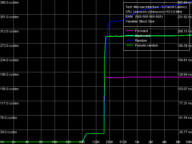
Picture 7. L1/L2 D-Cache and RAM Latency These curves (Picture 7) look typical of processors with an exclusive cache hierarchy. The most significant difference of Esther from Nehemiah, which we have already seen above, is the implementation of (for the first time in VIA processors) hardware prefetch, which is efficient in case of forward sequential memory walk. For example, a similar picture could be seen on AMD K7 processors. Table 6
Quantitative ratings of L1/L2 Cache and RAM latencies are published in Table 6. L1 Cache latency in the new Esther core remains on the level of 6 cycles, which first appeared in Nehemiah core (the previous generation of VIA C3 processors with Ezra/Samuel cores used to have 4-cycle L1 Cache). Thus, VIA processors still possess the highest L1 D-Cache access latency. "Average" L2 D-Cache latency of the new Esther core has also grown (that is the latency in normal conditions, without unloading the bus) — it's 4 cycles as high as in Nehemiah. Well, the changes are not unexpected, considering the significant changes in the cache structure - longer cache lines (64 bytes, which are more common now). RAM latency in the platform under review is very high — it's even higher than in the previously reviewed platform with VIA Antaur. A partial remedy to this situation is hardware prefetch for forward sequential memory access, which reduces the latency to 120 ns, while its true latency is demonstrated during backward and pseudo-random walks - 194 ns. As we wrote many times, a further increase in latency in random walk mode has to do with depleting D-TLB, which in this case can hold only 128 pages, that is it can cover an area of 512 KB, no more. Minimum Latency of L2 D-Cache/MemoryLet's rate the minimum L2 D-Cache latency of VIA C7-M processors by unloading L1-L2 bus with empty operations (Picture 8). 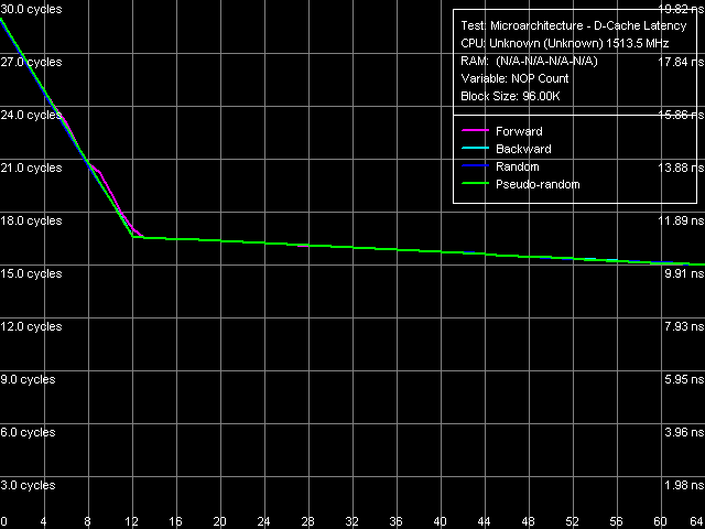
Picture 8. Minimum L2 D-Cache Latency For unknown reasons (it happens on all VIA processors), a preliminary test of measuring the execution time of single NOP gives an excessive result (in this case — about 1.03 cycles instead of 1.00), which leads to a lowering baseline as the number of NOPs, inserted between cache access commands, grows. Nevertheless, the error is relatively small in this case. It allows to see that the minimum latency in all cases is achieved, when 12 NOPs are inserted - 17 cycles. The same value (for 8 NOPs or more inserted) could be also seen on VIA Antaur (see Table 7). Table 7
We shall rate the minimum memory latency using a similar test, increasing the block size to 4 MB. 
Picture 9. Minimum RAM Latency A picture of the unloaded L2-RAM bus (Picture 9) resembles that for AMD K7 processors, where hardware prefetch is also implemented for forward sequential walks only and is of relatively low efficiency — the unload curve goes down very smoothly and does not reach its minimum even in case of 64 NOPs inserted. Minimum memory latency at this point is 94 ns. In case of backward, pseudo-random, random walks, the curves have a typical "saw-tooth" look at 15 NOP steps, which correspond to the FSB frequency multiplier (100 MHz x 15 = 1.5 GHz). As it usually happens, minimum latencies in these modes are not much different from their mean values. Data Cache AssociativityL2 Cache of the new Esther core has a very interesting peculiarity - very high 32-way associativity — VIA C7/C7-M models are currently the first processors with such a high-associativity cache (it's not quite clear why, considering its small capacity - just 128 KB). Let's try to determine L1/L2 D-Cache associativity of the processor under review using a standard test (Picture 10). 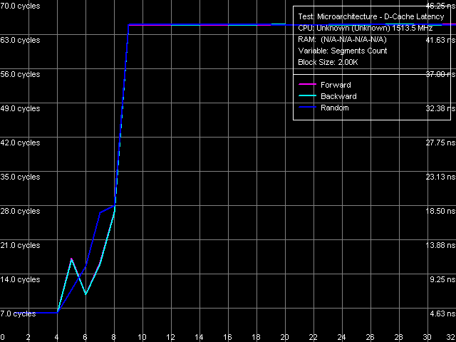
Picture 10. L1/L2 D-Cache Associativity Unfortunately, this test does not give a clear picture — according to its results, we can say that L1 Cache associativity equals four (the first inflection on the graph); but as the number of segments grows, the picture gets blurry. But that's not surprising — their maximum number in this test is limited to 32 (when this test was developed, there were no processors with such caches), while the second inflection in this case (exclusive organization) must be at the number of segments equal to the total associativity of L1+L2 Caches, that is 36. Well, we can only believe in 32-way associativity of L2 Cache in C7/C7-M processors. Later on we shall expand functionality of our test package. Real L1-L2 Cache Bus BandwidthConsidering the exclusive organization of L1-L2 D-Caches in Antaur and C7/C7-M processors, when each access to L2 Cache along with transferring data from L2 into L1 is accompanied by pushing the "sacrificed" line from L1 to L2, real L1-L2 bus bandwidth values, obtained in RMMA, were doubled (Table 8). Table 8
As is known from our previous analysis of VIA processors, the L1-L2 data bus in VIA Antaur is characterized by relatively low bandwidth — just 2.56 bytes/cycle, which might indicate just a 32-bit organization. Nevertheless, the arrival test from that review showed that the bus capacity was actually 64 bit, as reading adjacent elements in a single 32-byte cache line was not accompanied by additional latencies. The L1-L2 bus got much faster in the new Esther core — up to 4.4 bytes/cycle (a tad faster for writing than for reading — the same picture could be seen in the very first test, when we examined L2 Cache bandwidth for reading and writing). That's quite good actually, considering increased bandwidth requirements to this bus, imposed by the cache line increased to 64 bytes. At the same time, bus capacity still remains on the level of 64 bit, which is not that bad actually. The same situation (64-bit bus, 64-byte lines) can be seen in the AMD K7 architecture, for example. Let's use the arrival test (Picture 11) to confirm our assumption about the 64-bit L1-L2 bus. 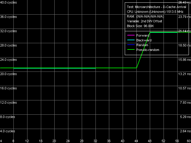
Picture 11. Data Arrival from L1-L2 Bus, Test 1 This test reads two elements from the same cache line, the second element being at a specified distance (4-60 bytes) from the first one (beginning of the line). This test shows that only the first 48 bytes (from 0 to 47 inclusive) arrive from L2 cache for 6 cycles of L1 Cache access, while a request of the following 48th byte is accompanied by a noticeable latency growth. It means that the data transfer rate is indeed 48/6 = 8 bytes/cycle, that is the bus capacity is 64 bit. Besides, the second variation of the arrival test (Picture 12) allows to learn additional details about the data arrival order from L2 to L1. 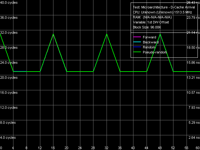
Picture 11. Data Arrival from L1-L2 Bus, Test 2 Offset of the first requested element from the start of the line is a variable is this test (from 0 to 60 bytes), while the second requested element is always shifted from the first one by -4 bytes (except for the initial point, when the offset equals -4 + 64 = +60 bytes, because both elements must be in the same cache line). The curves (Picture 12) show that data from L2 Cache of VIA C7/C7-M processors are read in 16-byte blocks. Data can be read from any 16-tuple position (maximum points on the curves):
A similar picture, but with 8-byte "granulation", is demonstrated by the AMD K7/K8 architecture, that is D-Cache organization in VIA processors is getting increasingly similar to that in AMD processors. I-Cache, Decode/Execute EfficiencyAt first, let's have a look at the situation with decoding/executing the simplest NOP instructions, because it's quite different from the typical picture (Picture 13). 
Picture 13. Decode/execute efficiency, NOP instructions That is there is no distinct area that corresponds to executing instructions from L2 Cache. It does not mean that L2 Cache of this processor "does not work" for caching code (instead of data), as decode/execute speed at 64-192 KB actually differs from that outside the total size of L1 and L2 caches. At the same time, the situation with decoding/executing other instructions, for example 6-byte compare operations cmp eax, xxxxxxxxh (CMP 3-6), is more typical (Picture 14). 
Picture 14. Decode/execute efficiency, CMP instructions Let's proceed to quantitative ratings of decode/execute speed in Table 9. Table 9
What concerns decoding/executing the simplest ALU operations (independent as well as pseudo-dependent) from L1 Cache, there have been no changes here since the first VIA C3 processors (probably even since earlier VIA/Centaur processors). Maximum decode/execution speed of these instructions remains on the level of one instruction per cycle, which is too slow for these days. Decode/execute speed of CMP 2 (cmp ax, 0000h) and Prefixed CMP 1-4 ([rep][addrovr]cmp eax, xxxxxxxxh) instructions is still lower compared to the other instructions. Their execution speed is slowed down as many times as there are prefixes together with the main operation. For example, the execution speed of CMP 2 is twice as low (1 prefix + 1 operation), while prefixed CMP instructions are executed three times as slow (2 prefixes + 1 operation). It means that like all previous VIA processors, processors on Esther core still spend their execution units on "executing" each prefix. Prefixed NOP Decode Efficiency test also corroborates this fact - it decodes/executes instructions of the following type: [66h]nNOP, n = 0..14 (Picture 15). 
Picture 15. Decode/execute efficiency for prefix instructions NOP Decode/execute efficiency of such instructions, expressed in bytes/cycle, does not depend on a number of prefixes and always equals 1 byte/cycle. It means that the execution time of a single instruction, expressed in CPU cycles, indeed grows linearly together with the number of its prefixes. This approach is quite inefficient, considering that prefixes are not that rare in x86 code (especially considering SSE/SSE2/SSE3 instructions, now supported by Esther core). I-Cache Associativity
Picture 16. I-Cache Associativity As in case with L1/L2 D-Cache associativity, I-Cache associativity test (Picture 16) demonstrates only the official L1 I-Cache associativity (4). The second inflection area that corresponds to the total associativity of L1 I-Cache and shared L2 I/D-Cache (36), just does not fit this graph. Let's hope to see it in future in a new RMMA version. Instruction Re-Order Buffer (I-ROB)Esther core demonstrates quite an interesting picture in I-ROB (Picture 17), which works like this: it runs one simple instruction that takes much time to execute (it uses an operation of dependent loading of a subsequent string from memory, mov eax, [eax], and right after it a series of very simple operations, which do not depend on the previous instruction (nop). Ideally, as soon as the execution time of this combo starts to depend on the number of NOPs, the I-ROB can be considered used up. 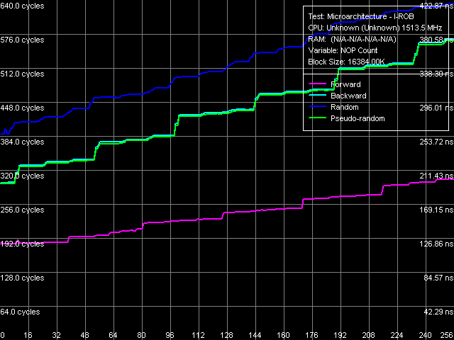
Picture 17. Instruction Re-Order Buffer Size What's interesting, execution time of this combo practically immediately starts depending on a number of NOPs. It means only one thing — VIA C7/C7-M processors lack the instruction re-order buffer, that is out-of-order code execution is out of the question for these processors. However, the lack of I-ROB blends well with the general picture of a simple CPU microarchitecture, like the above mentioned decoder and execution units. TLB Characteristics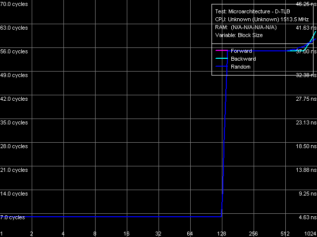
Picture 18. D-TLB size 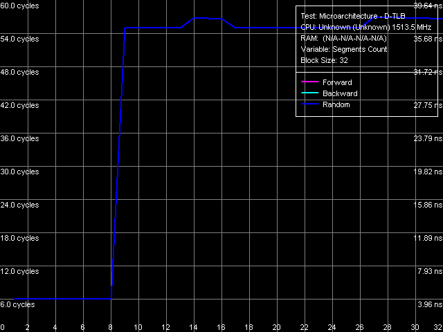
Picture 19. D-TLB associativity Like in case of Nehemiah core and unlike earlier models, tests of D-TLB size (Picture 18) and associativity (Picture 19) give no surprises. D-TLB size is indeed 128 entries (we saw it in CPUID characteristics as well as in the L1/L2/RAM latency test), the miss penalty (out of its limits) is very large — about 49 cycles. Associativity level is 8, associativity miss is accompanied by approximately the same penalty. 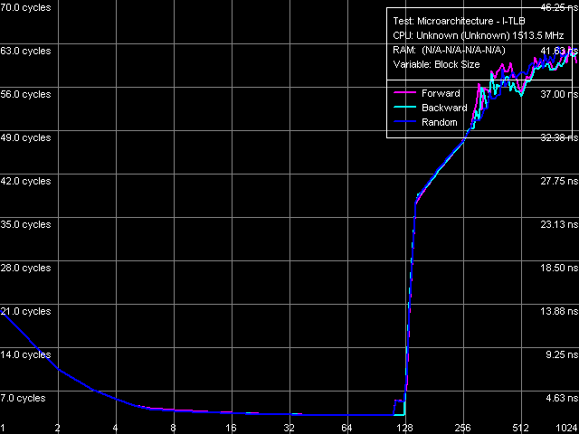
Picture 20. I-TLB size 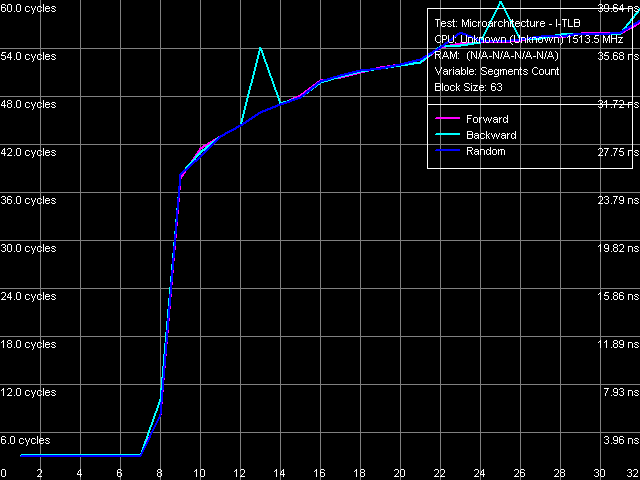
Picture 21. I-TLB associativity The above-said also applies to I-TLB tests — size (Picture 20) and associativity (Picture 21). I-TLB size is also 128 entries, its associativity level is 8. Besides, the initial area of the I-TLB size test allows to determine L1 I-Cache latency, that is execution time of a single unconditional short-range branch - 3 cycles. I-TLB miss penalty is more difficult to determine, because latency grows constantly together with the number of memory pages walked. But in both cases (size miss and associativity miss) we can determine an initial area, where latency grows to about 38-39 cycles, that is the minimum I-TLB miss penalty amounts to 35-36 processor cycles. ConclusionIn microarchitectural terms, the new Esther core of VIA C7/C7-M processors is not a break-through or something cardinally new. It's just a revision of the previous Nehemiah core in many respects — that core was used in desktop VIA C3 processors of the second generation and in mobile VIA Antaur processors. The most important differences of C7/C7-M from C3/Antaur apparent to the naked eye come down to support for SSE2 and SSE3 SIMD instructions, enlarging L2 Cache to 128 KB and raising its associativity level to 32, as well as (less evident for a common user) increasing line sizes of all caches to 64 bytes. While the memory system changes are quite successful — L1-L2 bus and L2 Cache bandwidths were increased, which in its turn allowed to achieve higher memory bandwidth and justified a faster V4 FSB (Pentium 4 Quad-Pumped bus counterpart); alas, we cannot say the same about computing units of the processors. VIA C7/C7-M processors still have a mediocre decoder, which cannot effectively process prefixed instructions — all SIMD instructions in particular. To all appearances, the number of execution unit was not changed either — at least even the simplest ALU operations are still executed at the speed of one operation per cycle. Thus, you can hardly expect high performance from the new VIA C7/C7-M processors. Even if we trust VIA advertising that these processors offer the best performance per Watt ratio compared to all other processors, it's quite clear that it's achieved solely due to their low power, not due to their high performance. So, the field of application of VIA processors is still limited to superlow-power solutions, which cannot offer high performance. Dmitri Besedin (dmitri_b@ixbt.com)
April 11, 2006 Write a comment below. No registration needed!
|
Platform · Video · Multimedia · Mobile · Other || About us & Privacy policy · Twitter · Facebook Copyright © Byrds Research & Publishing, Ltd., 1997–2011. All rights reserved. | ||||||||||||||||||||||||||||||||||||||||||||||||||||||||||||||||||||||||||||||||||||||||||||||||||||||||||||||||||||||||||||||||||||||||||||||||||||||||||||||||||||||||||||||||||||||||||||||||


