 |
||
|
||
| ||
|
||
|
||
| ||
December 14-15, 2005. A unique event, the first in the 30-year history of Intel in Israel — the first official press event for journalists and EMEA analysts, devoted to Intel's production and research centers in this country. Formally coincided with the start of Fab28 construction, this event was not timed to it, just a tour of Intel Israel. OverviewIntel's history in Israel starts from a foundation of an R&D center in Haifa in 1974 with just 5 employees. The Israeli division of Intel is currently the largest employer in the country and consists of five R&D centers in Haifa, Jerusalem, Kiryat Gat, Petach Tikva, and Yakum. Its staff is over 6000 employees. The top-priority line of Intel activity in Israel is R&D — Israeli division of Intel has been acting as a R&D center for Intel divisions all over the world for over 30 years. Among the achievements of the research center in Haifa and its divisions in Yakum and Jerusalem are the first PC processor with a 8-bit 8088 bus, Intel MMX and Intel Centrino. The development center in Petach Tikva plays a leading role in Intel Mobility Group since the first processor (codenamed Manitoba) for mobile phones designed in 2003. Day 1. Research centers in Haifa and Petach TikvaThe first day of the event was devoted to visiting research centers in Haifa and Petach Tikva. As we have already mentioned, research and development is the main Intel's line of activity in Israel. Research center in HaifaHaifa event was opened with presentations conducted by Vice President and Mobility Group CEO Dadi Perlmutter and Mobility Group Vice President Ron Friedman, devoted to the history of the development center in Haifa and Intel Centrino evolution. The research center in Haifa is the first Intel's design and development center, established outside the US and the only such center that combines various research lines — designing processors for mobile devices and PC, telecom equipment and software. 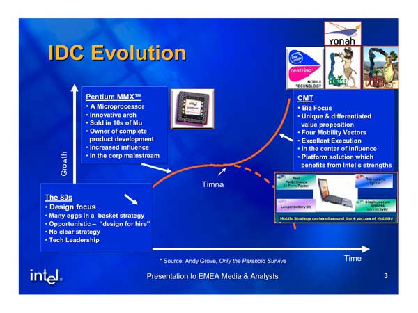 The history of this center can be divided into three stages. As you can see from the slide, the first stage (80s) did not have a well planned strategy. It was oriented mostly to design and development of new products. The main objective was to reach technical leadership. We cannot say that this approach was not successful — it led to the development of Intel Pentium MMX in mid 90s, which allowed this center to strengthen its hand inside the corporation. Further development resulted in a hump in the history of this center — a failed design of an integrated solution, codenamed Timna. 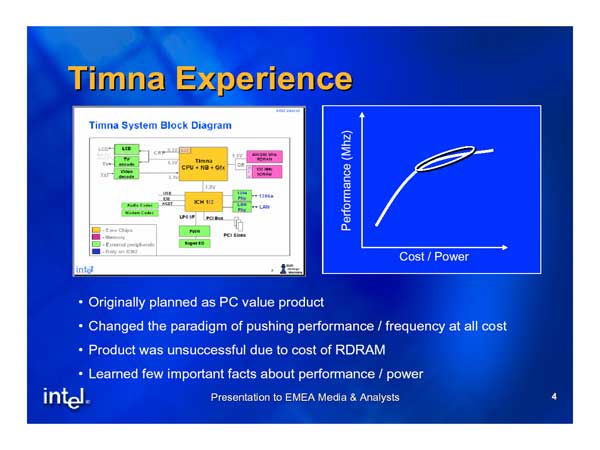 Timna was a processor, a northbridge, and a graphics controller, integrated in the same die, which was positioned as a mass solution for inexpensive PCs. Nevertheless, development of this solution faced some problems, the most important being a considerable increase in heat dissipation and cost of the end solution even at an insignificant increase in its clock above a certain threshold. The other reasons for the failure, which are not directly related to Timna design, include a high cost and the general lack of success of RDRAM memory, which was planned to be used in this solution. Nevertheless, Timna failure led to important consequences for the research center strategy — it learned a few important facts about performance / power. In this connection, the paradigm of pushing performance / frequency at all cost suffered cardinal changes. Thus started the third "biz focus" stage, which led to the development of the well-known Centrino platform. Development strategy of the first 130-nm Pentium M core, a key Centrino component codenamed Banias, consisted in (1) passing from the "performance" notion to the "power per a performance unit" notion (interestingly, after several years Intel glided back to importance of this parameter, but only to its contrary notion — "performance per Watt"). The second factor for Banias development was the emphasis on reducing active and inactive power consumption — that is the power consumed both under heavy load as well as in idle mode. This approach suffered practically no changes in the development of the second generation of Centrino, based on 90-nm Dothan core. Speaking of the further development of the mobile platform, the presentation touched upon (as far as possible) Yonah and Merom processors. 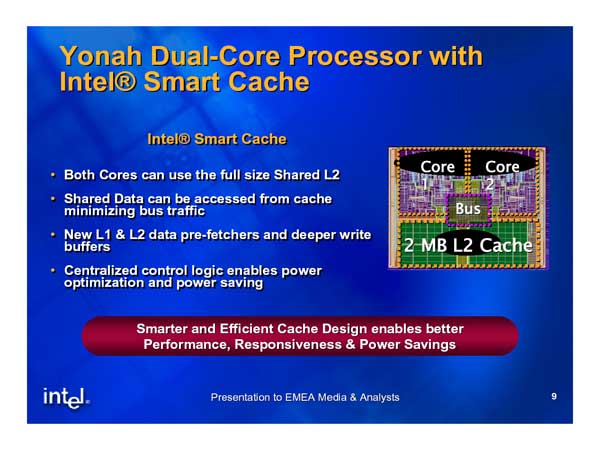 A very important feature of the recently announced dual core Yonah is Intel Smart Cache technology. It consists in efficient usage of a shared L2 Cache by both processor cores without using an external system bus as well as a more efficient data prefetch from L1/L2 Caches of a processor. Besides, centralized control logic of L2 Cache inside a processor enables power optimizations in cache usage. As is known, L2 Cache often takes up a larger part of a die and contributes much into the overall CPU power consumption. In this connection, power saving tasks include (1) disabling unused cache sections but retaining integrity and data coordination between the cache and memory (this technology has been used in Pentium M since Banias times). The second in the list, but not in importance, is a technological task to reach minimum possible cache voltage (Vcc_Min) without losing data stability. In Yonah, these problems are solved by three technologies: Intel Smart Cache, Enhanced Intel Deeper Sleep, as well as low-Vcc design of the data cache. In conclusion, the presentation about Centrino evolution provided some facts about the IA-32 architecture of the next generation, which will be used in Merom (mobile processor), Conroe (desktop processor), and Woodcrest (server processor). These processors have been mentioned many times during various Intel events, starting from IDF in San-Francisco in August 2005. This time we were given a brief list of the key features, namely:
Presentation of the research center in Haifa ended in the following interesting statements:
After the presentation, we had a one-hour tour of the research center, where we could learn the history of the center in photos since its foundation as well as its current activities. Along with purely intellectual projects, the center is into testing and fine-tuning products on the die level. The center possesses equipment both for destructive and non-destructive methods of fault analysis. The most impressive part is its capacities for fixing faults by modifying ready dice, which looks like "point-to-point wiring". Judge for yourself: we saw the following practical demonstration (not in real time though) - two wrong tracks on a die were cut, covered with several atomic layers of tungsten, and then new correct tracks were created. Such an approach (consecutive cycles of tests and adjustments) allows to find and fix several technological faults in CMOS devices at once. Thus, it significantly saves expenses compared to the situation when these faults are detected and fixed one-by-one by manufacturing new versions of a die. Research center in Petach TikvaThe R&D center in Petach Tikva was presented by its CEO Erez Schwartz. Its presentation was devoted to mobile telecom devices. The center was founded in 1999 together with the acquisition of DSPC. The main objectives of the center is to design hardware and software platforms and to optimize mobile handheld devices "from antenna to applications". Cellular & Handheld Group specializes in designing so-called multi-radio devices that support several different telecommunications standards (for example, usual mobile phones supporting GSM/GPRS and Bluetooth). The staff numbers about 850 engineers, who have more than 15 years of experience in wireless technologies and mobile telecommunications. 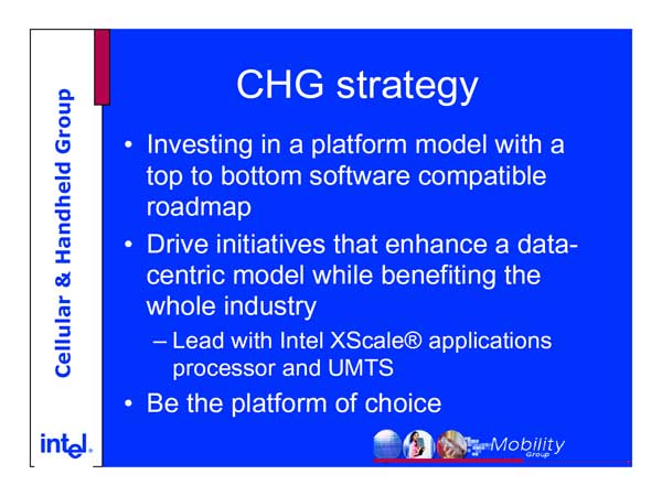 What is the strategy of Cellular & Handheld Group? First of all, it's investing in a platform model with a top to bottom software compatible roadmap. We speak of designing complex applications that can be easily ported from the high-end segment into entry-level segments, which is possible thanks to the unified platform architecture. The second initiative is a datacentric model. It means promoting ideas that convince users of the necessity to use their mobile phones not only for voice communication, but also as a data transfer tool. For this purpose, attractive applications should be created to urge end users to use data services. And finally, no less important is the objective to be a "platform of choice", which requires launching good solutions and offering good tech support. The second line of activity of the R&D center is to design, test, and introduce WiMAX solutions. This topic was covered in the presentation by Dan Eldar, Deputy CEO of Intel WiMAX Group. 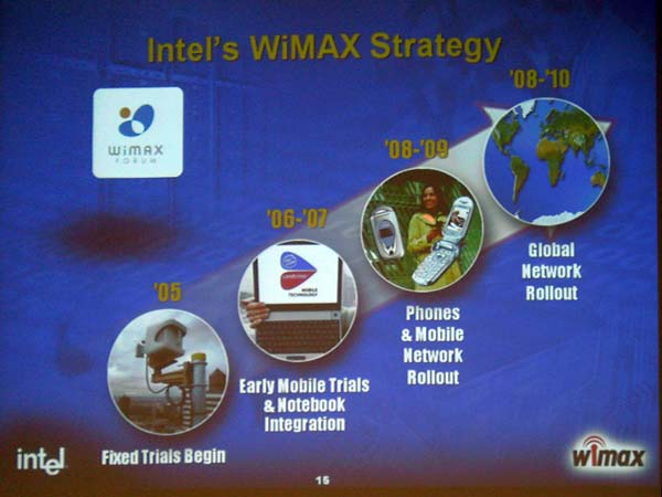 Intel corporation has been actively mentioning WiMAX during its various events since 2004. The first fixed trials of WiMAX became an important event in 2005. Intel's plans for the nearest future (2006-2007) include early mobile trials and notebooks integration. Further development (2008-2009) implies WiMAX introduction into mobile phones and deployment of the first WiMAX networks — 4G mobile networks. The strategy ends in a global WiMAX network rollout in 2008-2010. Well, we shall see how WiMAX will develop in real life. Day 2. Production plants in Kiryat Gat and JerusalemProduction plants in Kiryat Gat — Fab 18 and Fab 28The second day of the event, devoted to Intel production plants in Kiryat Gat and Jerusalem, was opened by the presentation of Vice President of Technology and Manufacturing Group and Israeli CEO Alex Kornhauser. The lecturer provided basic information about Intel divisions in Israel. The title — There’s a part of Intel in every part of the world — is not coincidental, as it reflects the role of Intel Israel as one of large contributors into research and development of Intel products all over the world. 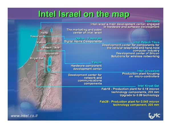 Intel presence in Israel numbers five R&D centers and three production plants (two of them are working already, one is still under construction). The main development center is situated in Haifa. The marketing and sales center is also headquartered here. As we have already mentioned above, Intel's history in Israel started from the foundation of this center in 1974, as the first Intel's R&D center outside the United States. The next development center (if we move from the North to the South) in Yokne'am, was founded in April-May 2005 in connection with Oplus acquisition. It's currently one of the main development centers working on digital home solutions (image and video processing software, LCD technologies). Yakum houses a division of Intel's development center in Haifa. One of the reasons for founding this center was in depleted manpower in the North of the country. So it was decided to found a new center in the central part of the country instead of attracting potential employees from the central part of the country into the northern part — R&D center in Haifa. In 1999 Intel made an important $1.6mlrd acquisition - DSPC became a research center for mobile and wireless communications (including WiMAX) in Petach Tikva. Intel divisions in Jerusalem are represented by a production plant and an R&D center. Fab 8 was founded in 1985 and was the first Intel's plant outside the United States. Fab 8 production is based on 6" (150mm) silicon wafers — Fab 8 is the last Intel's 6" plant, as the other facilities are switched to the new 12" (300mm) standard. Key products from this plant are microcontrollers for automotive industry (in particular, Bosch is one of the main Fab 8 clients). Besides, Fab 8 currently includes a research center for MEMS and semiconductor photonics (details below). Aside from Fab 8, there is a separate development center in Jerusalem, which was bought in 1998 as part of a local R&D DEC division. The last but not the least is Fab 18 in Kiryat Gat, which manufactures early models of Pentium III and Pentium 4 processors as well as 0.18-micron chipsets. Today this production plant is being reconstructed for the 90-nm process technology. It promises to become one of the main suppliers of 90-nm flash memory. Besides, on December 1st Intel announced a construction of a new plant (Fab 28) — the second plant for manufacturing 45-nm components. Speaking of Intel finances in Israel, the overall export since 1974 is over $12 mlrd, export growth for the last year is over $1 mlrd. Intel's total investments (apart from acquisitions) are about $3 mlrd, expected investments into the Fab 28 construction will bring another $3.5 mlrd by the end of 2009. Intel is the main private investor in the country. Several words about new Fab 28. As we have already mentioned above, Fab 28 will manufacture 45-nm microelectronic components with 300-mm (12") silicon wafers. Cleanroom area of this production plant will be 20000 m2, which is more than twice as large as the cleanroom in Fab 18. Production lines will be launched in the second half of 2008. Approximately 2000 new employees will be hired (Intel Israel will grow to 8-9 thousand employees). The expected export of the production plant should be about $3 mlrd a year. Nevertheless, let's return to existing Fab 18, which was presented by Vice President of Technology and Manufacturing Group Maxine Fassberg. Fab 18 is currently the largest Intel production plant in Israel, its staff numbering 3700 people. The total investments into the Fab 18 construction is about $1.8 mlrd, the plant was launched in the first half of 1999. 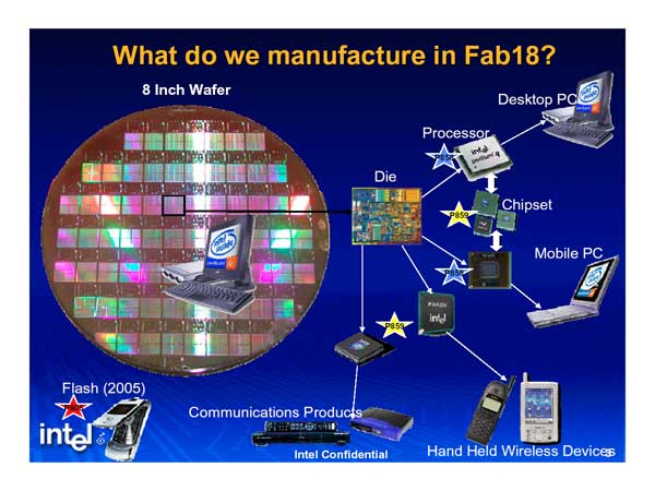 Fab 18 products were initially manufactured by 0.18-micron process technology - mostly logic devices, including dice for early Intel Pentium III and Pentium 4 models. As Intel's microprocessing industry switches to 0.13-micron process technology, Fab 18 was reequipped for 0.18-micron chipset production. These days a considerable part of products from this plant are processors for PDAs and modern mobile phones. Besides, in 2005 the company initiated the process of switching the plant to 90-nm process technology, based on copper (the two generations older 0.18-micron process was based on aluminum). It's also reoriented to manufacturing flash memory. After the presentation we had an excursion around Fab 18 - cleanroom (as it's not allowed to enter this room without special clothes, we could only look through the windows) and operations department, where ready products (reference platforms) are thoroughly tested (including the latest Yonah) in different (normal and abnormal) conditions. 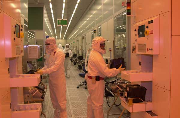 Production plant in Jerusalem — Fab 8Jerusalem Fab 8 presentation was conducted by its CEO Yonathan Wand. As we have already mentioned, Fab 8 was the first production division of Intel, established outside the USA in 1985. Fab 8 is a relatively small plant — both in terms of area (Fab 8 cleanroom area is just 4500 m2, which is twice as small as in Fab 18) as well as employees (about 500 people). Fab 8 is a consolidating plant — it manufactures all legacy products from Intel. It offers six process technologies (see the table), which is very difficult in technological terms (typical Intel production employs no more than 1-2, very rarely three processes). Hence a wide product line — over 100 products, manufactured in small quantities.
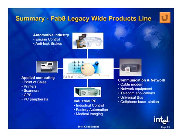 Fab 8 manufactures a lot of legacy products. The main consumer of these products is the automotive industry. Fab 8 is the only Intel's plant that manufactures automotive products — Anti-lock Brake Systems (ABS) and engine controls. The clients are leading world manufacturers of the first echelon — Bosch, Ford, Siemens, and Motorola. It also manufacturers solutions that combine microcontrollers and flash memory. In this case, the consumer of such solutions, called Electronic Stability Program (ESP), is Bosch. The second type of products is 51-series (8-bit) and 96-series (16-bit) microcontrollers, which are used in commercial and industry solutions — Point of Sales, industrial control, medical equipment, telecom devices. Such products are ordered both by OEM companies (Nortel, Lucent, Ericsson) as well as distributors (Arrow, Avent, Hamilton). Strange as it may seem, the next line of products is x86 processors of the three generations — 186, 386, and 486. These processors, manufactured by this plant in large quantities in the past (for example, Fab 8 manufactured up to 50% of the total volume of 386 processors) and being the heart of personal computers, are now manufactured in small quantities and are used in POS, modems, GPS solutions due to their reliability and utility. That's why consumers of x86 products from this plant are the leading companies - IBM, NEC, and Garmlin. And finally, we shouldn't forget about Intel's presence on the RISC-processors market. i960-series processors in several modifications with various performance levels are used in network solutions, telecom equipment, and printers. Nokia, Cisco, Alcatel, and HP consume RISC-solutions from Intel. 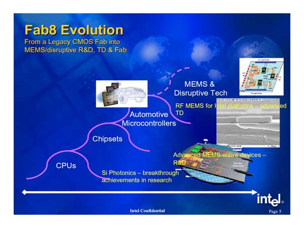 For its twenty-year history, Fab 8 passed three main stages — from manufacturing processors to manufacturing chipsets and automotive microcontrollers. Nevertheless, Fab 8 is not just a manufacturing division of Intel. Approximately five years ago, the next evolution stage took shape — Fab 8 management initiated the search for new unusual technological solutions. These days Fab 8 is the main and only R&D center of unique disruptive technologies, such as MEMS and semiconductor photonics. Israel Yankovich conducted a presentation of the first of these technologies. What is MEMS? This abbreviation stands for Micro-Electro-Mechanical Systems: "Micro" means small dimensions of elements (about 0.5-1 micron, but not smaller — this is one of the reasons to design such devices exactly in Fab 8); "Electro-Mechanical" means the importance of both electric and mechanical properties; "Systems" implies MEMS integration with other chips. MEMS is sometimes called MST — Micro Systems Technology. 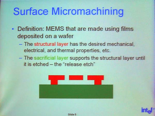 One of the methods to manufacture MEMS is surface micromachining. This method consists in consecutively applying films (layers) on the silicon wafer and subsequent processing. There are two layer types: (1) the structural layer has the desired electrical, mechanical, and thermal properties; (2) the sacrificial layer. This layer is the first to be deposited. It supports the structural layer until it's etched and then it's removed from a wafer. 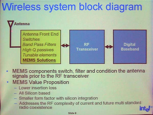 The key application of MEMS is wireless devices. In the wireless system block diagram above, MEMS can act as a pre RF unit, which contains band pass filters, amplifiers, tunable elements, etc. MEMS advantages lie in using silicon to make all components of the system, that is the best integration, which leads to smaller form factors, better performance, and low power consumption. 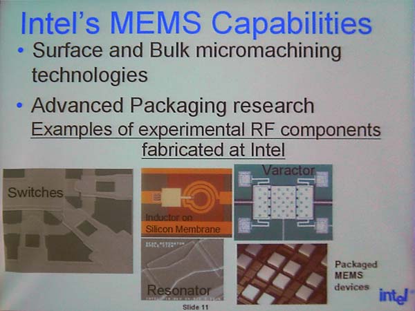 The slide shows experimental MEMS components, which are currently designed and fabricated: electronic switches, inductors, resonators, varactors. The main problem of manufacturing MEMS devices is their packaging. Usual chip-production methods are obviously unsuitable for MEMS packaging. First of all, fragile MEMS structures must be protected from destructive processes, such as wafer splitting into dice and cleaning. Secondly, MEMS packaging must be done immediately after etching a substrate layer — otherwise some particles may get into the etched cavities and seal mechanical units. Thirdly, cavities in MEMS devices imply complete impermeability of packaging. In this connection, the least expensive approach to MEMS manufacturing is to package devices on the level of entire silicon wafers instead of individual chips. The second line of research in the R&D department of Fab 8 is semiconductors or silicon photonics. It was presented by Nahum Izhaky. Photonics is a technology of emitting, transferring, controlling, and detecting photons using principles similar to those in optical fibre and optoelectronic devices. Advantages of using optical technologies for data transfer lie in miniature dimensions and simplicity of such devices (using a few signal lines), absolute insensibility to electromagnetic interference, low losses at long-range transmissions even of high theoretical throughput (up to 100 TB/s). Nevertheless, they are not without drawbacks, high costs in the first place due to exotic and expensive materials (gallium arsenide, indium phosphide, etc), expensive manufacturing and packaging technologies. In this connection, Intel sees its semiconductor photonics task in developing CMOS-compatible photonics — photonic devices based on usual silicon and standard streamlined technologies for semiconductor production in large volumes in the existing plants. Even though Si integration into photonics offers some problems, as silicon does not have some necessary properties like electro-optic effect and effective photon emission, Intel's research and development in this area has made great progress since the first Raman-effect continuous silicon laser designed in 2004. 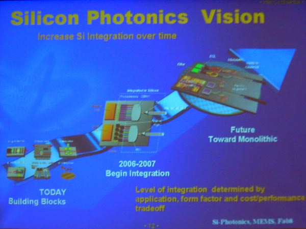 Photonic device development is currently at the building blocks stage — emitter, waveguide, modulator, radiation detector, as well as their packaging and control. In the nearest future (2006-2007) the corporation plans to start integrating building blocks with a prospect of designing monolithic devices. Solution of this task will require efficient methods of testing photonic devices on the silicon wafer level, economic packaging and integration of photonic devices with regular CMOS solutions, which will allow to go from pilot to large-scale production of such devices.
Dmitri Besedin (dmitri_b@ixbt.com)
February 2, 2006. Write a comment below. No registration needed!
|
Platform · Video · Multimedia · Mobile · Other || About us & Privacy policy · Twitter · Facebook Copyright © Byrds Research & Publishing, Ltd., 1997–2011. All rights reserved. |


