 |
||
|
||
| ||
|
||
|
||
| ||
VIA Apollo KT 266 - how to warm up the peopleVIA Technologies has very competently prepared the people for a release of their DDR-chipset for Socket A. Look how beautifully they have done it: First, ALi announced in a loud voice that they were first to release a chipset for DDR SDRAM, and there were two chipsets at the same time: for Pentium III, and for AMD Athlon. All motherboard manufacturers immediately launched their solutions (primarily on the ALi MAGiK 1). VIA was silent. Although everybody knew that they were going to release Apollo Pro266 and Apollo KT266, VIA didn't specify the release date. After that the manufacturers started reporting about some problems of the ALi MAGiK 1, and the boards were called back for redesign. VIA was still keeping silence. I wish I knew a real reason - was it just a physical unreadiness of the product, or a deliberate marketing policy, I don't know, but the second variant seems to be completely possible. Then it was AMD's turn to report about a mass production of the AMD-760. The manufacturers started announcing their solutions again, and VIA Technologies still said nothing. The companies encountered problems with the design and stability of the boards once again, that time it was with the AMD-760. At last, a DDR-chipset from VIA appeared on the scene, but it wasn't a long-awaited KT266 - but only Apollo Pro266. All hardware-testers doubted of high results due to the processor bus of the Pentium III. The assumptions were fair, but nevertheless, the VIA Apollo Pro266 was one of the most efficient chipsets for Socket 370" platform. And a final touch. I'm sure that too low results of the KT266's performance published by some sites which had been received on the supposedly "beta-versions" of the motherboards, were faked-up. Are we going to live with an expensive and scare AMD-760 which supports nothing except the DDR memory, and with a cheap, universal but slow ALi MAGiK 1?! Final. Testing of the VIA Apollo KT266 in our lab :) VIA Apollo KT266 as a DDR-platform from VIA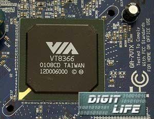 The chipset for the DDR SDRAM for a Socket A platform (AMD Athlon/Duron) is a real flagship for the whole DDR-platform from VIA. Having taken the EV6 processor bus, AMD was looking farther ahead. Now the bus of the Athlon/Duron processors has turned to be the best for all possibilities of Double Data Rate. And it is not surprising since the bus is based on a DDR-like technology. At the rated frequency of 100 MHz, the EV6 has a bandwidth equivalent to 200 MHz for a usual bus. At 133 MHz its bandwidth increases as much as 266 MHz. It means that the data rate of the most efficient PC2100 DDR SDRAM completely corresponds to the bandwidth of the processor bus of the latest Athlons. And what about Pentium III? This processor is at the tail-end: the fast DDR SDRAM makes no sense when 133 MHz AGTL+ is incapable to deliver data to the processor at least at the same rate at which data come from the memory. But it is not worth burying the DDR SDRAM on the Intel platform, since the Pentium 4 has 400 MHz Quad-Pumped FSB - it is more than the fastest DDR-memory can give today. VIA Apollo KT2661. General view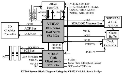 The chipset consists of two chips: VT8366 System Controller (North Bridge (NB)) and VT8233 V-Link South Bridge (SB). The system controller has at the least the following functions:
By the way, which functional blocks should be placed in the north or in the south bridge is determined with respect to a bandwidth required for the given interface. All high-speed interfaces (a system bus, AGP, a memory bus) are realized in the north bridge, others (IDE, USB etc.) are brought to the south bridge. Moreover, some very slow interfaces (COM, LTP-ports) are realized as separate additional controllers. Now only SIS uses chipsets where NB and SB are located in one chip. This approach has both advantages (a low prime cost of the chipset, a possibility to expand very much a bandwidth between a north and a south bridge or to connect IDE directly to the north bridge, a possibility to produce compact boards) and downsides (it is difficult to make a competent lay-out for such a complex chip). With increase in a digit capacity or in the number of memory buses or in case of the Quad-Pumped Bus (for Pentium 4), a lot of new outputs will be added to this chip. In this case no serious designing problems shall arise, but the manufacturers will have to migrate to more expensive 6-layer PCBs. Another important component of the system controller is a memory bus controller. This interface is a stumbling block in an endless struggle of VIA and Intel. While Intel has always the higher performance, VIA is ahead as far as a volume of memory supported and functionality are concerned (the number of RAM types with which a chipset can work). 2. Memory controllerThe DRAM controller of the KT266 chipset supports all available technologies and it is strange that RDRAM is not supported. The controller supports PC66, PC100 and PC133 SDRAM, VCM SDRAM, as well as PC1600 and PC2100 DDR SDRAM. For the unbuffered SDR/DDR modules 6 memory banks with possibility to install up to 3 GBytes are supported (3 double-side memory modules with 16 512Mbit chips allow to reach such a volume), and for the Registered SDR/DDR modules 8 banks with up to 4 GBytes are supported. The ECC support allows to correct single-bit and to reveal multi-bit errors, what is important for highly reliable systems. When SDRAM is used usual modules easily get on with VCM, moreover, the controller allows to set timings for each bank separately. The memory interface can work both synchronously with FSB, and at the frequency 33 MHz more and less than the processor bus frequency, irrespective of a memory type used. It means that the Athlon with 200 MHz bus can be used both with PC100 SDR and PC1600 DDR memory, and with PC133 SDR and PC2100 DDR. On the contrary, in a system with 226 MHz Athlon the chipset allows to use PC100 SDR and PC1600 DDR modules, though it was developed as a High-End solution and it is rational to use it with PC2100 DDR SDRAM and 266 MHz AMD processors. Let's see what the developers have done to achieve the maximum performance. First, support of 8 interleave memory banks means that 8 pages can be open in order to reduce an access time. The banks are selected according to the LRU algorithm (last recently used). Secondly, buffers of recording from CPU into DRAM and buffers of reading from DRAM into CPU (which consist of 4 cache lines (16 quadwords) each) are used. Besides, there are such additional features as an intellectual processing of instructions for more uniform load of a memory bus (for example, a preliminary preparation of other banks during reading from the current bank), an advance reading for continuous loading the CPU with data etc. 3. Processor busThe EV-6 bus controller was developed the most carefully, it is an analog of those which are used in KT133 and KT133A. The Athlon/Duron processors for Socket-462 and with 200 and 266 MHz bus are supported, but apart from this well-known fact there are much deeper and more interesting features. As you know, data, address and instruction buses are independent. So, the controller contains a queue of 4 entries, a probe queue that keeps 4 entries with requests of the system to a processor, and a big queue of interface control instructions (24 entries) which provide a continuous data stream via EV-6 bus consisting of record and read buffers. Such buffering ensures a complete load of the bus and minimal delays. 4. AGP and V-Link controllersThe AGP controller is compatible with AGP v2.0 and supports 1X, 2X and 4X modes and SideBand Addressing (SBA). If a processor bus frequency is 133 MHz, the 66 MHz AGP and CPU works synchronously, and if it is 100 MHz they work in a pseudo-synchronous mode. The controller provides an uninterrupted operation by two queues for requests - a 32-level one for requests for reading and a 4-level one for requests for recording, and by two FIFO buffers - 256 byte capacity for reading data and 128 byte capacity for recording data. The sequence of requests can be changed to balance the load. By the way, such intellectual mechanism is used in a controller of the processor bus. The controller of the NB-SB bus provides 66 MHz V-Link interface with a peak bandwidth equal to 266 MBytes/s. The V-Link protocol is optimized for decreasing delays, but on the other hand, it estimates a size of transactions and a degree of a buffer load in order to prevent an overload. Due to integrated bus-to-bus bridges and a solid pipelining all north bridge controllers can work simultaneously and independently. The north bridge is implemented in a 552-pin BGA case, it is based on the 0.35 micron technological process and is intended for 3.3V power supply. It measures 35x35 mm and, on the whole, looks great 5. South bridgeNow I want to give you some interesting information on the VT8233 V-Link Client controller south bridge which is widely available since it is used together with a north bridge in the VIA Apollo Pro266 chipset. The internal structure of the bus of this controller is based on the 66 MHz PCI. The VT8233 south bridge contains the following functional blocks - a client interface for communication with the north bridge, a PCI controller and an LPC controller (low pin count). 5 PCI slots and a separate LPC bus are supported. There is a possibility to set a priority for a PCI device to minimize delays. Furthermore, 4 buffering levels allow to distribute a PCI bus load as effectively as possible. As you can see, our table of DDR-chipsets with all key features of south and north bridges is getting wider.
Gigabyte 7VTXSpecification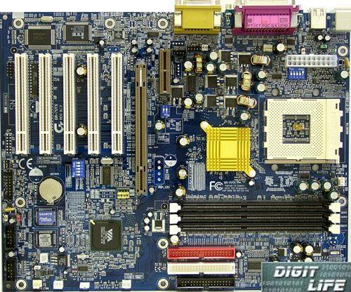
 The board with its performance and stability is much better than many production samples. The greatest contribution was made by Gigabyte R&D team. The 7VTX board allows to change a processor's frequency from BIOS within the following ranges: 100-128, 133-160, 166-180 MHz in 1 MHz increments. For frequencies higher than 166 MHz the divisor 1/5 on the PCI is used to receive frequencies close to the rated 33 MHz and higher, and 2/5 on the AGP is used to obtain 66 MHz and higher. Besides, there are DIP-switches for a forced change of the multiplier, for increase of voltage of the memory and AGP - a great deal of possibilities as compared with a useless soft EasyTune! The board is not a production sample, and in the box you can find only FDD cables, a 80-conductor IDE cable, and a disc with drivers. Production revisions usually start from 1.xx. But anyway, we are glad that this sample performed so well. BoardAt first sight a standard ATX size (30.5x24 cm) may seem to be too big for the 7VTX mainboard - it lacks for an external IDE controller which takes too much space with two IDE connectors. But on the other hand, such size is preferable for ATX cases - the third row of mounting holes is right on the edge of the board, and the board won't bend when FDD and IDE cable are connected. Stability of the board is perfect - it has passed quite successfully a 24-hour Stress-testing under Windows 2000 Professional. All this has become possible due three-phase supply which is able to feed Athlon processors with frequencies up to 1.5 GHz. It may seem that 13 1200uF capacitors are not enough, but it is unimportant with three-phase supply. The capacitors are placed so that they wouldn't prevent installation of big coolers. The side of the Socket where coolers are snapped is turned to an external edge of the board; it allows easy installation of them and brings to nought a risk of damaging the die. The board has AGP Pro slot, though in the current version a 12 V power connector is not unsoldered. But I'm sure that in production samples it will be as it should be. Three connectors for DDR SDRAM DIMMs are located quite conveniently - nothing prevents arranging memory modules even in the completely assembled system. All connectors are placed ideally - ATX-power connector is situated behind the socket but not too close to the board's edge, IDE/FDD connectors are not too close to each other, - it allows easy connection of the corresponding cables, internal connectors for audio devices are located next to external audio-outs. On a blue piece of textolite all connectors and switches are marked. Besides, you can find there a table which shows how switch positions correlate with processor multipliers and FSB frequencies. Plus, there is a well-known DualBIOS. 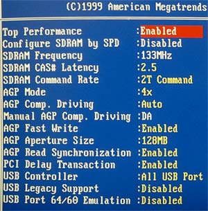 The BIOS is based on the AMI BIOS v1.24 and offers a lot of settings. I just don't understand what the Top Performance option is doing here. Besides, I wish there were an option for manual setting of "interleave". However, there is a possibility to choose DRAM command rate. I managed to boot the system with command rate = 1T and ran the Quake3 at 640X480X16 Fast. The result was 192.3 fps against 185.7 fps at command rate = 2T. PerformanceBefore testing I want to discuss some facts concerning this part and changes brought in in the test systems and software. First of all, DDR now shows not only acceptable but very good stability and performance. It concerns not only AMD 760 based systems but also ALi Magik 1 based ones and today the only tested KT266 system. The results of the ALi Magik 1 chipset will be shown in the next review. Now we can recommend you mainboards on all DDR chipsets provided that all boards on the newest KT266 are also good and reliable as the 7VTX board. Secondly, do not worry if you don't see a supposed 15% increase on the graphs. Note that the system based on the KT133A with SDRAM was tuned for the maximum performance - there were minimal memory timings and a 4-bank interleave. Today the problem lays in the DDR memory: the technology of production is not mastered well enough, and the memory works at the rated CAS2.5 at the breaking point. Let's estimate what will be a performance increase of the DDR system when all manufacturers supply a real DDR - PC2100 CAS2 with a good overclockability. Today such modules are delivered only by NANYA and Apacer. Well, the first way is to migrate from CAS2.5 memory to CAS2 memory, what will give 2-4% increase for the whole system. The second way is to set interleave modes of the memory, i.e. a possibility to keep up to 8 pages open at the same time against 4 ones in case of SDRAM. It will give 3% over. By the way, in the BIOS of the Gigabyte board this possibility is not realized yet. Another method can be used only with north bridges of VIA KT266 and Pro266. It is a possibility of manual adjusting delays when the chipset and the memory are exchanging instructions - DRAM command rate. This technology is a response to the Super Bypass from AMD. The new feature is supported by BIOS in the 7VTX. However, the Super Bypass from AMD and DRAM command rate from VIA are different - the AMD's technology relates to a chipset and doesn't depend on temporary parameters of the memory, whereas the command rate is directly connected with it. That is why we enabled Super Bypass for the tests and the command rate was set at default - 2T (2 time steps). The DRAM command rate 1T will allow the KT266 to outperform or at least to become equal with the AMD760. The performance must increase by 2-3%. Considering DDR systems with regard to the KT133A, I should note that we can receive those 15-20 % of the performance increase if we add a theoretical performance increase (which will be obtained with a full-value DDR memory) with those 7-10% we we have got now. In order to diminish an influence of the video subsystem on the test results we use an up-to-date video adapter (Ultimate Solution) based on the NVIDIA GeForce3, the core of which works at 200 MHz, with 64 MBytes 460 MHz DDR memory. The processor we use is the latest AMD Athlon Thunderbird with frequency of 1.33 GHz. The test system is:
Software:
Game applicationsApart from old bothersome games today we have a newcomer - the 3DMark 2001, which has managed to become legendary. We used the 3Dmark at 1024x768x32x100Hz with Hardware TCL enabled. 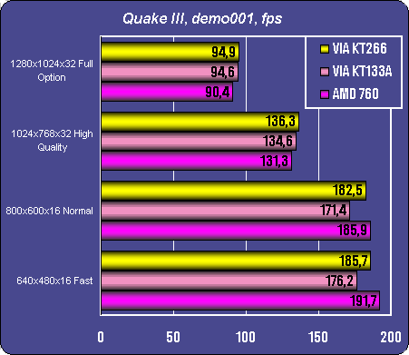 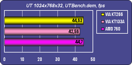 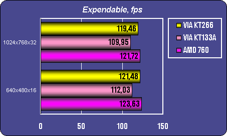 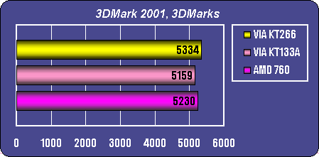 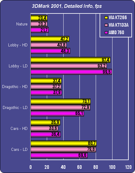 The AMD760 chipset copes not very well with AGP texturing - the system doesn't like when the AGP bus is loaded much, it is clearly seen, for example, in the Quake3 at 1280x1024x32. But on the other hand, the processor bus controller and the AMD761 memory controller are interacting more effectively due to the Super Bypass mode. It becomes apparent when transmitting from Low Detail to High Detail in the 3Dmark. It is interesting that in case of the Quake 3 an increase of the detailing level makes the KT266 a leader, and in case of the 3DMark 2001 the leader is the AMD760. It is simple to explain: in Quake3 in Full Options mode the most part of the load is accounted for by an increased volume of textures and a necessity of effective operation of the AGP. In the 3DMark 2001 the texture volume remains the same, while the number of polygons is getting bigger, as well as calculations of trajectories etc. In the KT266 chipset it is vice versa: AGP is realized perfectly, and interaction of the processor and the memory is a bit poorer. But do not forget the DRAM command rate, it should help the KT266 to take a leading position in games. The results of the AMD760 and KT266 look not so impressive as compared with the KT133A. Now again, if you add 7-8% to the KT266 results in Quake3 at 640X480X16 Fast, you will see that 200fps will be easily reached (earlier only the Pentium4 based systems could do that). Performance in graphics and multimedia applications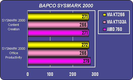 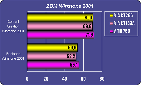 In the SYSmark 2000 Internet Content Creation the KT266 goes on a par with the AMD-760, sometimes coming ahead (Elastic Reality, Bryce), sometimes falling behind (Premiere, Photoshop). By the way, the both programs where the VIA chipset lags behind are from Adobe :) As you know, Adobe programmers has an interesting point of view about software writing - their methods can't be considered to be standard as far as Wintel-systems are concerned. Apparently, they do it to unify their programs in order they can be used for different platforms (x86 and Apple). It is worth noting that the KT133A together with usual PC133 SDRAM lags not too far behind. Besides, sometimes the SDRAM-chipset manages to win from the DDR AMD-760 chipset, though it is impossible for it to win from the KT266. It means that the new chipset from VIA Technologies is much better than the older one. The KT266 takes everything from the DDR, and if it is impossible to win, it just shows the same results as the KT133A + PC133 SDRAM does. Performance in business applicationsAs I have already mentioned, the Super Bypass technology can give a considerable performance gain in some cases. Note that a peculiarity of software of this class consists in the large number of jumps inside the code. And any possibility to reduce delays when applying to the memory looks excellent, in this case the Super Bypass function is a such possibility. 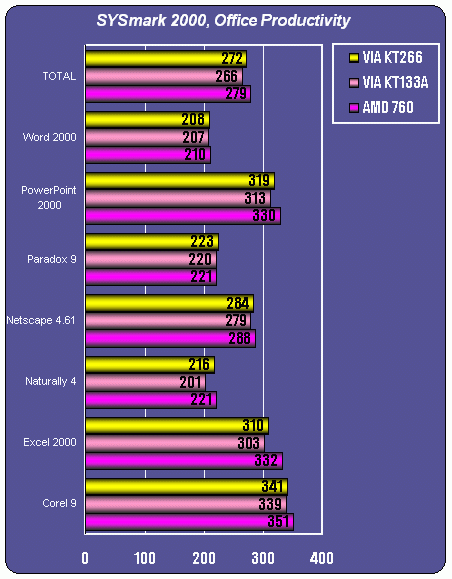 Our hero has unfortunately lost in the business applications. But don't pay too much attention to this fact, since "a computer performance in the Word 2000" sounds funny :) Performance in professional OpenGL applications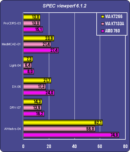 Professional applications for visualization of 3D graphics in real time mode, gathered in the SPEC viewperf test, seem to be created specially for the AMD760, it is the only type of applications where the KT266 falls behind significantly. The Super Bypass shines here as well. On the one hand, the huge number of primitives, the overdraw value, calculation of lighting etc., which allow to use the "processor-memory" bus very effectively, make the AMD760 a leader, and on the other hand, a small number of textures doesn't allow the KT266 to realize AGP in full. To estimate performance of the systems in 3Dstudio we used the Waterfall file. We implemented rendering of frames from 0 to 10. With the AMD Athlon 1.33 GHz it took 20-25 sec for each frame. The results are shown in seconds: the less, the better. 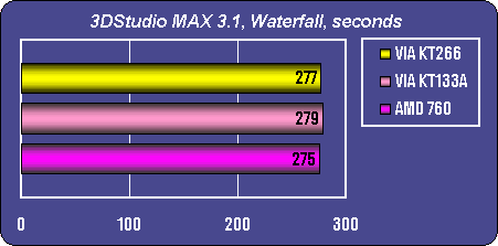 In this case the memory subsystem performance affects nothing, and the coprocessor is the only completely loaded part of the system. If your PC is intended only for rendering, you'd better buy more RAM than increase its bandwidth. ConclusionThe VIA Apollo KT266 has turned to be quite successful. The best advantage lies in wide possibilities for adjusting different parameters. The board is a perfect tool which allows to use all possibilities of the modern rapid PC2100 DDR SDRAM and of new AMD Athlons with 266 MHz system bus. Apart from the PC1600/PC2100 DDR SDRAM the KT266 supports a usual PC100/PC133 memory. Of course, the first boards on this chipset won't have slots for the old memory. However, in the future motherboards with support for memory of the two types will undoubtedly appear. The performance of the KT266 is adequate as compared with the AMD-760. If the AMD chipset is a bit "straightforward" (it supports only DDR, the memory controller is completely synchronous), the VIA chipset is more "elegant". In our opinion, the new chipset is a very good
solution which combines a cheap price, universality (what is untypical
for the AMD-760) and a good performance level (what the ALi MAGiK
1 is lacking for). Such a balance is a key advantage of the VIA
Apollo KT266, and it will help it to find its user very quickly.
Write a comment below. No registration needed!
|
Platform · Video · Multimedia · Mobile · Other || About us & Privacy policy · Twitter · Facebook Copyright © Byrds Research & Publishing, Ltd., 1997–2011. All rights reserved. |


